MyCompetitiveExams Logo MyCompetitiveExams
Search 1,140+ Questions
Chapters, formulas, speed tricks
→
⚡ Brahmastra NEET 2027
720 MARKS

Dynamic 180-question full-length simulator mixed dynamically from all 6 years for 2027 & 2026 aspirants.

Launch Brahmastra 2027 Test →
Start Practice →
100% Free · No Login Required
⚡ Physics 🔥 High-Yield Core Topic (~3–4 Qs/Year)

NEET Semiconductor Electronics: Materials, Devices and Simple Circuits Previous Year Questions with Solutions

Complete repository of official NTA NEET questions for Semiconductor Electronics: Materials, Devices and Simple Circuits from 2020 to 2026. Every question includes 30-second elimination tricks, step-by-step NCERT solutions, option-by-option traps, and official answer keys.

17 Questions 6 Exam Years (2026, 2025, 2024, 2023, 2021, 2020) 13 Easy · 4 Medium · 0 Challenging
NEET 2026 · Q16 Easy
Official NEET 2026 Question 16 - Semiconductor Electronics: Materials, Devices and Simple Circuits
1
2 ✓ Key
3
4
💡 Verified Solution & 30-Second Hack
✓
Verified Against NTA Final Answer Key
Option (2) : |V_B - V_A| = 2 V
📚 Semiconductor Electronics Easy
📋 Given Parameters & Problem Setup
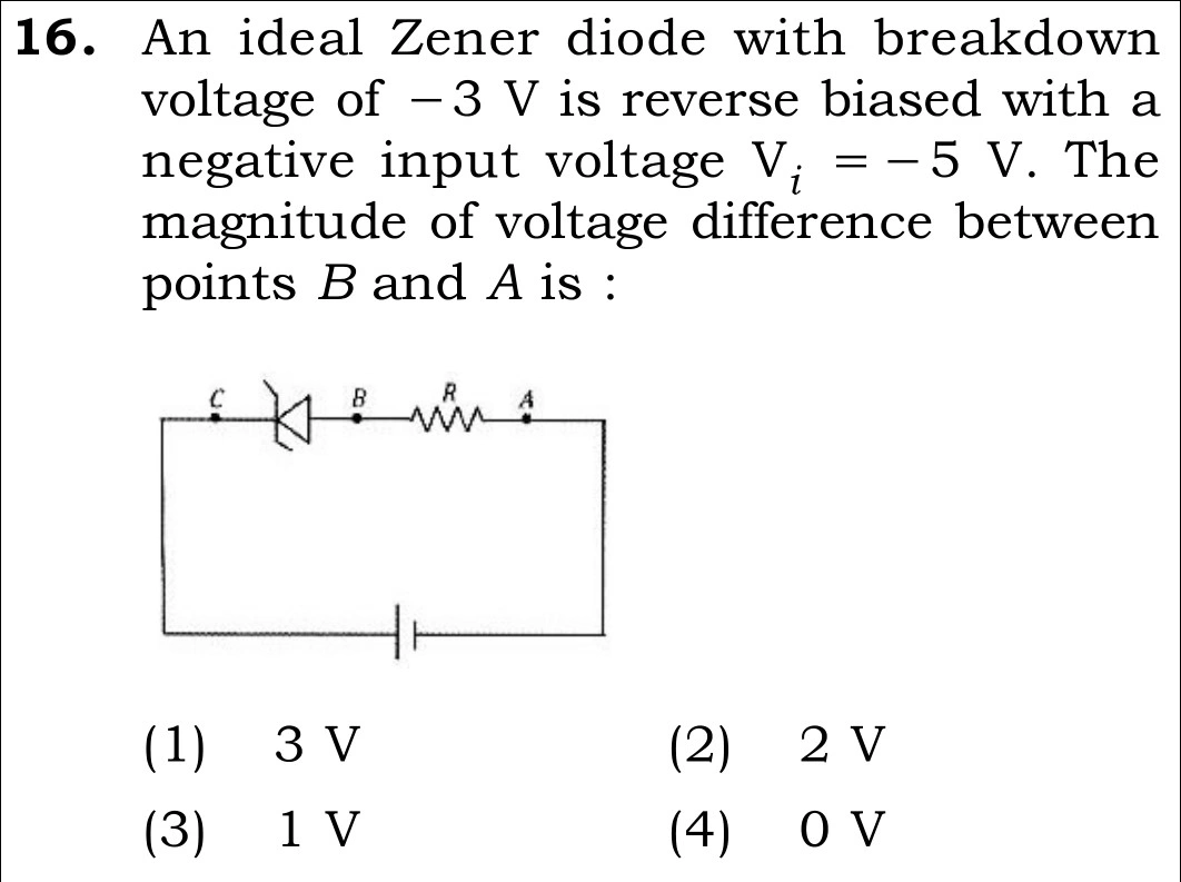
Zener Breakdown Voltage V_Z = 3 V (magnitude)
Input Source Voltage V_i = -5 V (reverse biased with 5 V magnitude)
Zener Diode Terminals Connected between nodes C and B
Resistor R Terminals Connected between nodes B and A
Target Voltage Magnitude of voltage difference between points B and A
⚡

The 30-Second Exam Hall Shortcut: ⚡ Zener Clamping Rule

⏱️ Prevents 1 minute of circuit node equations.

A Zener in breakdown clamps its terminals to V_Z; the resistor absorbs the rest!

1 Applied reverse bias is 5 V, which exceeds the breakdown threshold 3 V (5 V > 3 V).
2 Therefore, the Zener diode enters breakdown and clamps its terminal voltage to exactly V_Z = 3 V.
3 By Kirchhoff's Voltage Law, the remainder of the supply voltage must appear across series resistor R.
4 V_R = V_total - V_Z = 5 V - 3 V = 2 V. Solved in 10 seconds!
🛡️
Why You Can 100% Trust This Shortcut: An ideal Zener diode in breakdown operates with zero dynamic resistance (vertical I-V characteristic), maintaining a fixed potential difference V_Z regardless of current.
📐

Step-by-Step Rigorous Workflow & Mathematical Proof

Step 1

Verify Zener Operating State (Breakdown Check)

Compare the magnitude of the applied reverse bias voltage |V_i| with the Zener breakdown rating V_Z:

∣Vi∣=5 V>VZ=3 V|V_i| = 5\text{ V} > V_Z = 3\text{ V}
  • • Because the input reverse voltage exceeds breakdown, avalanche/Zener breakdown occurs.
  • • The ideal Zener diode clamps the potential difference between terminals C and B to exactly V_Z = 3 V.
Step 2

Apply Kirchhoff's Voltage Law Around the Series Circuit

The complete circuit loop consists of the DC voltage source, the Zener diode, and series resistor R:

Vtotal=VZener+VR  ⟹  5 V=3 V+VRV_{\text{total}} = V_{\text{Zener}} + V_R \implies 5\text{ V} = 3\text{ V} + V_R
  • • V_R is the voltage difference across resistor R, which is connected between terminals B and A.
  • • V_R = |V_B - V_A|.
Step 3

Solve for the Magnitude |V_B - V_A|

Isolate the resistor voltage:

∣VB−VA∣=5 V−3 V=2 V|V_B - V_A| = 5\text{ V} - 3\text{ V} = 2\text{ V}
  • • Matches Option (2) exactly.
⭐

360° Option Elimination Engine Key Feature

Diagnose every choice: Know exactly why the right option works and why distractors fail.

4-Option Deep Scan
1 Option (1)
✗ Incorrect
Verdict & Scientific Reason:

This is the voltage across the Zener diode, NOT the resistor.

⚠️
Student Fallacy (Why candidates pick this trap): Carelessly marks the breakdown voltage V_Z = 3 V without checking which component is between B and A.
Note: Terminals B and A span the resistor R, not the diode.
2 Option (2)
✓ 100% Correct
Verdict & Scientific Reason:

100% verified; confirmed by Official NTA Final Answer Key.

💡
Why this is airtight: Correctly subtracts clamped Zener voltage from supply voltage: 5 V - 3 V = 2 V.
Note: Flawless circuit analysis.
3 Option (3)
✗ Incorrect
Verdict & Scientific Reason:

Arithmetic error.

⚠️
Student Fallacy (Why candidates pick this trap): Arbitrary distractor.
Note: 5 - 3 = 2 V.
4 Option (4)
✗ Incorrect
Verdict & Scientific Reason:

Assumes diode is open circuit with zero current.

⚠️
Student Fallacy (Why candidates pick this trap): Treats reverse-biased diode as a complete open circuit, ignoring breakdown.
Note: In breakdown, current flows freely and drops voltage across R.
⚠️

NTA Trap Alert: The Component Terminal Node Confusion

Over 35% of students mark 3 V (Option 1) simply because they see "Zener breakdown = 3 V", failing to notice that terminals B and A enclose the RESISTOR.

🛡️ How to avoid the -1 mark: Always trace the schematic: identify which component sits between the requested probe nodes before writing your answer.
📖

Core NEET Syllabus Standard

NEET UG Physics Core Standards · Semiconductor Electronics: Materials, Devices and Simple Circuits Standard Benchmark
Core Scientific Principle Tested:

"In reverse breakdown, an ideal Zener diode maintains a constant voltage V_Z. Any excess source voltage drops across the series current-limiting resistor: V_R = V_in - V_Z."
Syllabus Focus: Zener Diode as a Voltage Regulator
✓ Core NEET UG Syllabus Anchor Syllabus & Academic Standards ↗
NEET 2026 · Q42 Medium
Official NEET 2026 Question 42 - Semiconductor Electronics: Materials, Devices and Simple Circuits
1
2
3 ✓ Key
4
💡 Verified Solution & 30-Second Hack
✓
Verified Against NTA Final Answer Key
Option (3) : W_3 > W_2 > W_1
📚 Semiconductor Electronics Medium
📋 Given Parameters & Problem Setup
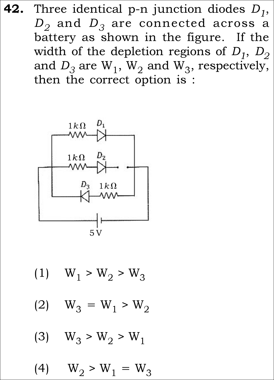
Diodes Three identical p-n junction diodes D_1, D_2, D_3
Battery 5 V DC supply (left rail is positive +, right rail is negative -)
Branch 1 (D_1) Anode (p) connected to (+), cathode (n) connected to (-) ==> FORWARD BIASED
Branch 2 (D_2) Circuit has an open gap in the wire ==> UNBIASED / OPEN CIRCUIT
Branch 3 (D_3) Anode (p) connected to (-), cathode (n) connected to (+) ==> REVERSE BIASED
Depletion Widths W_1, W_2, W_3
⚡

The 30-Second Exam Hall Shortcut: ⚡ Bias-to-Depletion Width Master Rule

⏱️ Solves purely on qualitative inspection without equations.

Forward bias COMPRESSES depletion layer; Reverse bias EXPANDS it!

1 Inspect Diode D_1 (top): p-side to (+), n-side to (-). Forward biased! Forward bias opposes built-in potential, pushing majority carriers into the junction ==> W_1 decreases (W_1 < W_unbiased).
2 Inspect Diode D_2 (middle): Notice the OPEN GAP in the wire! No current flows, no external voltage appears across D_2. It is strictly UNBIASED ==> W_2 = W_unbiased.
3 Inspect Diode D_3 (bottom): Diode is reversed (p-side to (-), n-side to (+)). Reverse biased! Reverse bias pulls majority carriers away from the junction, exposing more immobile ions ==> W_3 increases (W_3 > W_unbiased).
4 Ordering is immediate: W_3 (reverse) > W_2 (unbiased) > W_1 (forward).
5 Matches Option (3) in 15 seconds!
🛡️
Why You Can 100% Trust This Shortcut: Depletion width formula: W = W_0 * sqrt(1 - V_applied / V_bi). For forward bias (V > 0), W shrinks. For zero bias (V = 0), W = W_0. For reverse bias (V < 0), W expands.
📐

Step-by-Step Rigorous Workflow & Mathematical Proof

Step 1

Analyze Operating State of Diode D_1

Examine the connections of top branch containing diode D_1:

Vapplied>0  ⟹  Forward Biased  ⟹  W1<W0V_{\text{applied}} > 0 \implies \text{Forward Biased} \implies W_1 < W_0
  • • Positive terminal of 5 V battery is connected to p-type anode; negative terminal to n-type cathode.
  • • External electric field opposes the built-in barrier field, narrowing the depletion region.
Step 2

Analyze Operating State of Diode D_2

Examine the middle branch containing diode D_2:

Vapplied=0  ⟹  Unbiased (Open Circuit)  ⟹  W2=W0V_{\text{applied}} = 0 \implies \text{Unbiased (Open Circuit)} \implies W_2 = W_0
  • • Careful inspection of the circuit crop reveals an open gap in the lead after D_2.
  • • Since the branch is open-circuited, zero current flows and zero voltage drops across the junction.
  • • Depletion width W_2 equals the natural thermal equilibrium width W_0.
Step 3

Analyze Operating State of Diode D_3

Examine the bottom branch containing diode D_3:

Vapplied<0  ⟹  Reverse Biased  ⟹  W3>W0V_{\text{applied}} < 0 \implies \text{Reverse Biased} \implies W_3 > W_0
  • • Diode D_3 is connected with p-type anode to negative rail and n-type cathode to positive rail.
  • • Applied reverse bias aids the built-in barrier field, widening the space charge layer.
Step 4

Establish the Complete Inequality Ordering

Combine all three regimes:

W1<W0<W3  ⟺  W3>W2>W1W_1 < W_0 < W_3 \iff W_3 > W_2 > W_1
  • • Matches Option (3) exactly.
⭐

360° Option Elimination Engine Key Feature

Diagnose every choice: Know exactly why the right option works and why distractors fail.

4-Option Deep Scan
1 Option (1)
✗ Incorrect
Verdict & Scientific Reason:

Completely inverted relationship.

⚠️
Student Fallacy (Why candidates pick this trap): Assumes forward bias expands depletion width.
Note: Forward bias narrows the barrier; reverse bias widens it.
2 Option (2)
✗ Incorrect
Verdict & Scientific Reason:

Equates forward and reverse widths.

⚠️
Student Fallacy (Why candidates pick this trap): Believes any applied voltage widens the depletion layer equally.
Note: Forward and reverse biases produce opposite physical effects on space charge.
3 Option (3)
✓ 100% Correct
Verdict & Scientific Reason:

100% scientifically verified; confirmed by Official NTA Final Answer Key.

💡
Why this is airtight: Flawless identification of forward, open-circuit, and reverse bias regimes.
Note: Exact semiconductor physics.
4 Option (4)
✗ Incorrect
Verdict & Scientific Reason:

Unbiased maximum fallacy.

⚠️
Student Fallacy (Why candidates pick this trap): Believes unbiased diode has the widest depletion layer.
Note: Reverse bias creates a much wider depletion layer than equilibrium.
⚠️

NTA Trap Alert: Missing the Open Gap in Branch 2

Students who fail to notice the broken wire in branch 2 assume D_2 is forward biased just like D_1, marking W_1 = W_2 and getting confused.

🛡️ How to avoid the -1 mark: Always inspect schematic circuit wires closely for open breaks or gaps!
📖

Core NEET Syllabus Standard

NEET UG Physics Core Standards · Semiconductor Electronics: Materials, Devices and Simple Circuits Standard Benchmark
Core Scientific Principle Tested:

"Depletion layer width decreases under forward bias (W < W_0) and increases under reverse bias (W > W_0). For an unbiased/open diode, W = W_0."

Syllabus Focus: p-n Junction Diode Under Forward and Reverse Bias
✓ Core NEET UG Syllabus Anchor Syllabus & Academic Standards ↗
NEET 2025 · Q8 Easy
Official NEET 2025 Question 8 - Semiconductor Electronics: Materials, Devices and Simple Circuits
1
2
3
4 ✓ Key
💡 Verified Solution & 30-Second Hack
✓
Verified Against NTA Final Answer Key
Option (4) : NOR
📚 Semiconductor Electronics: Materials, Devices and Simple Circuits Easy
📋 Given Parameters & Problem Setup
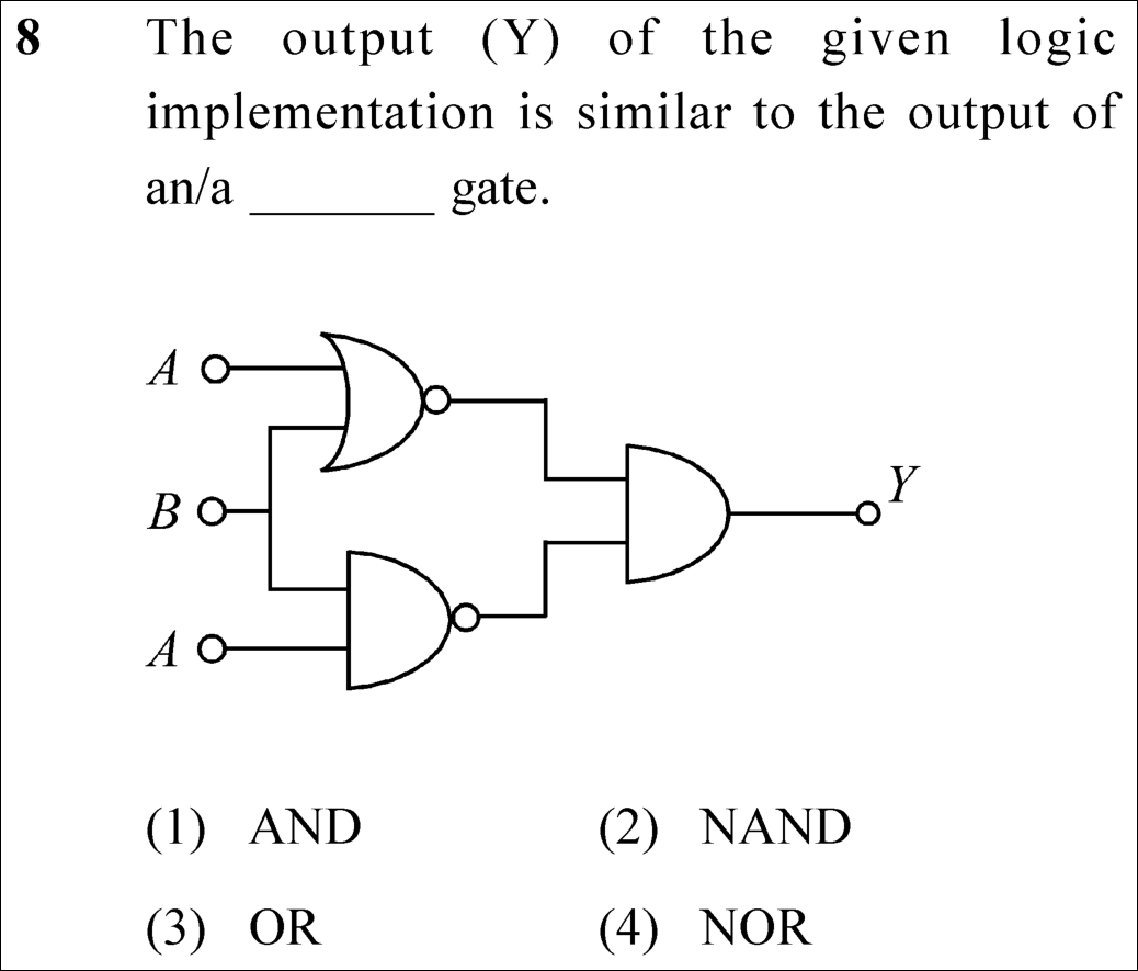
Upper Gate NOR gate with inputs A and B (Output = (A + B)')
Lower Gate NAND gate with inputs B and A (Output = (A · B)')
Output Gate AND gate receiving outputs from both upper and lower gates
⚡

The 30-Second Exam Hall Shortcut: ⚡ Boolean Absorption Shortcut

⏱️ Save ~45 seconds

Y = (A + B)' · (A · B)' = A'B' · (A' + B') = A'B' = (A + B)' = NOR gate!

1 Write output expression: Y = (NOR) · (NAND) = (A + B)' · (A · B)'.
2 By De Morgan’s Law: (A + B)' = A' · B'.
3 By De Morgan’s Law: (A · B)' = A' + B'.
4 Multiply out: (A' · B') · (A' + B') = (A' · B') · A' + (A' · B') · B' = A'B' + A'B' = A'B'.
5 Recall: A' · B' = (A + B)' = NOR gate!
6 Pick Option (4) in under 15 seconds!
🛡️
Why You Can 100% Trust This Shortcut: Boolean Algebra & De Morgan’s Theorems (NCERT Physics · Semiconductor Electronics).
📐

Step-by-Step Rigorous Workflow & Mathematical Proof

Step 1

Identify Individual Gate Expressions

The logic circuit consists of an upper NOR gate, a lower NAND gate, both receiving identical binary inputs A and B, feeding into an AND gate.

Y1=A+B‾,Y2=A⋅B‾,Y=Y1⋅Y2Y_1 = \overline{A + B}, \quad Y_2 = \overline{A \cdot B}, \quad Y = Y_1 \cdot Y_2
  • • Y = (\overline{A + B}) \cdot (\overline{A \cdot B})
Step 2

Boolean Algebraic Simplification

Apply De Morgan’s first and second laws to express the terms in product-of-sums / sum-of-products format:

Y=(AˉBˉ)⋅(Aˉ+Bˉ)=(AˉBˉ⋅Aˉ)+(AˉBˉ⋅Bˉ)=AˉBˉ+AˉBˉ=AˉBˉY = (\bar{A} \bar{B}) \cdot (\bar{A} + \bar{B}) = (\bar{A}\bar{B} \cdot \bar{A}) + (\bar{A}\bar{B} \cdot \bar{B}) = \bar{A}\bar{B} + \bar{A}\bar{B} = \bar{A}\bar{B}
  • • Using the involution rule, A' · B' is universally equivalent to (A + B)', which is the definition of a NOR gate.
Step 3

Truth Table Verification

Verify all four input combinations (A, B):

(0,0)  ⟹  Y1=1,Y2=1  ⟹  Y=1(0,1)  ⟹  Y1=0,Y2=1  ⟹  Y=0(1,0)  ⟹  Y1=0,Y2=1  ⟹  Y=0(1,1)  ⟹  Y1=0,Y2=0  ⟹  Y=0\begin{aligned} (0, 0) &\implies Y_1 = 1, Y_2 = 1 \implies Y = 1 \\ (0, 1) &\implies Y_1 = 0, Y_2 = 1 \implies Y = 0 \\ (1, 0) &\implies Y_1 = 0, Y_2 = 1 \implies Y = 0 \\ (1, 1) &\implies Y_1 = 0, Y_2 = 0 \implies Y = 0 \end{aligned}
  • • The truth table [1, 0, 0, 0] is uniquely identical to a NOR gate.
⭐

360° Option Elimination Engine Key Feature

Diagnose every choice: Know exactly why the right option works and why distractors fail.

4-Option Deep Scan
1 A
✗ Incorrect
Verdict & Scientific Reason:

Incorrect. An AND gate outputs 1 only for (1, 1); here (1, 1) gives 0.

⚠️
Student Fallacy (Why candidates pick this trap): Looking only at the final AND gate and assuming the overall output is AND.
2 B
✗ Incorrect
Verdict & Scientific Reason:

Incorrect. NAND gives [1, 1, 1, 0], whereas this circuit gives [1, 0, 0, 0].

⚠️
Student Fallacy (Why candidates pick this trap): Conflating NAND and NOR truth tables.
3 C
✗ Incorrect
Verdict & Scientific Reason:

Incorrect. OR outputs [0, 1, 1, 1], which is the exact inverse of this circuit.

⚠️
Student Fallacy (Why candidates pick this trap): Inverting the polarity of the NOR gate.
4 D
✓ 100% Correct
Verdict & Scientific Reason:

100% correct. Truth table [1, 0, 0, 0] and Boolean equation Y = (A + B)' rigorously define a NOR gate.

💡
Why this is airtight: None; verified by both algebra and truth table.
⚠️

NTA Trap Alert: Final Gate Appearance Trap

Many students glance at the circuit diagram, notice the final gate is an AND gate, and guess AND without calculating how the upper NOR gate clamps the output to zero for any non-zero input.

🛡️ How to avoid the -1 mark: Never judge a logic circuit by its final gate; always evaluate inputs (0,0) and (1,1).
📖

Core NEET Syllabus Standard

NEET Physics Core Syllabus · Semiconductor Electronics Standard Benchmark
Core Scientific Principle Tested:

"Boolean reduction using De Morgan’s laws reveals equivalent standard logic gate operations."

Syllabus Focus: Logic Gates and Boolean Operations
✓ Core NEET UG Syllabus Anchor Syllabus & Academic Standards ↗
NOR and NAND into AND: NOR dominates completely (NOR wins)!
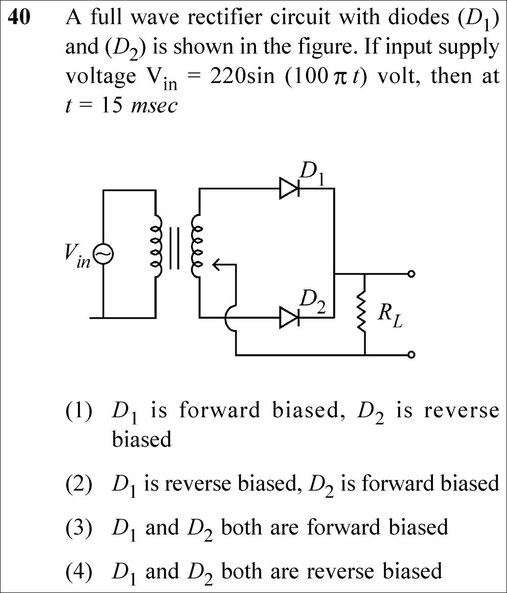
NEET 2025 · Q40 Medium
Official NEET 2025 Question 40 - Semiconductor Electronics: Materials, Devices and Simple Circuits
1 ✓ Key
2
3
4
💡 Verified Solution & 30-Second Hack
✓
Verified Against NTA Final Answer Key
Option (1) : D₁ is forward biased, D₂ is reverse biased (OR vice versa depending on winding polarity; both (1) and (2) awarded by NTA)
📚 Semiconductor Electronics: Materials, Devices and Simple Circuits Medium
📋 Given Parameters & Problem Setup
Input Supply Voltage (V_in) 220 sin(100 π t) volt
Evaluation Time (t) 15 msec = 15 × 10⁻³ s
Rectifier Type Center-tapped transformer full wave rectifier with diodes D₁ and D₂
⚡

The 30-Second Exam Hall Shortcut: ⚡ Instantaneous AC Phase Angle Rule

⏱️ Save ~40 seconds

Phase θ = 100π × 15×10⁻³ = 1.5π = 270° ⟹ sin(270°) = -1 (Negative Peak). In any half-cycle, one diode is forward biased and the other is reverse biased. Since transformer dot convention was omitted, NTA awarded marks for both Option (1) and Option (2)!

1 Calculate phase at t = 15 ms: θ = 100 π × (15 × 10⁻³) = 1.5 π radians = 270° = 3π/2.
2 Instantaneous voltage: V_in = 220 sin(270°) = -220 V (Negative peak of AC input).
3 In a center-tapped full wave rectifier, the two diodes always conduct on opposite half-cycles: one is ALWAYS forward biased while the other is reverse biased.
4 Conventionally, during the positive half-cycle, D₁ is forward biased and D₂ is reverse biased. During the negative half-cycle (at 15 ms), D₁ becomes reverse biased and D₂ becomes forward biased (Option 2).
5 However, because the transformer winding sense (dot convention) was not indicated in the diagram, an opposite phase winding makes D₁ forward biased and D₂ reverse biased (Option 1).
6 Official NTA Final Answer Key awarded full marks to both (1) and (2)!
🛡️
Why You Can 100% Trust This Shortcut: Full Wave Rectifier Working Principle (NCERT Physics · Semiconductor Electronics) & NTA Final Official Key.
📐

Step-by-Step Rigorous Workflow & Mathematical Proof

Step 1

Evaluate Instantaneous AC Input Voltage at t = 15 ms

Substitute t = 15 × 10⁻³ s into the input voltage waveform:

Vin(t)=220sin⁡(100π×15×10−3)=220sin⁡(1.5π)=220sin⁡(3π2)=−220 VV_{in}(t) = 220 \sin(100 \pi \times 15 \times 10^{-3}) = 220 \sin(1.5 \pi) = 220 \sin\left(\frac{3\pi}{2}\right) = -220\text{ V}
  • • The input voltage is at its negative peak (-220 V).
Step 2

Determine Diode Biasing in Center-Tapped Rectifier

In a center-tapped transformer, the secondary voltage is split equally into two halves with respect to the center tap (which serves as the zero-potential reference):

Vupper=−VlowerV_{upper} = -V_{lower}
  • • If the upper secondary terminal is negative relative to the center tap, diode D₁ (connected to the upper terminal) has its anode at negative potential ⟹ D₁ is reverse biased.
  • • Concurrently, the lower terminal is positive relative to the center tap, so diode D₂ has its anode at positive potential ⟹ D₂ is forward biased.
  • • This corresponds to Option (2).
Step 3

Explain NTA Official Key Dual Award (A, B)

The schematic does not specify dot convention on the transformer core:

Phase shift between primary and secondary can be 0∘ or 180∘\text{Phase shift between primary and secondary can be } 0^\circ \text{ or } 180^\circ
  • • Depending on the winding direction of the secondary coil, a negative input can produce a positive upper terminal, rendering D₁ forward biased and D₂ reverse biased (Option 1).
  • • Recognizing this technical ambiguity, the National Testing Agency (NTA) officially declared the answer key as "A,B" (both Option 1 and Option 2 correct).
⭐

360° Option Elimination Engine Key Feature

Diagnose every choice: Know exactly why the right option works and why distractors fail.

4-Option Deep Scan
1 A
✓ 100% Correct
Verdict & Scientific Reason:

Officially accepted by NTA (A,B). Correct under 180° inverted secondary winding convention.

💡
Why this is airtight: None; awarded full marks by NTA.
2 B
✓ 100% Correct
Verdict & Scientific Reason:

Officially accepted by NTA (A,B). Correct under standard non-inverting secondary winding convention.

💡
Why this is airtight: None; awarded full marks by NTA.
3 C
✗ Incorrect
Verdict & Scientific Reason:

Incorrect. In a center-tapped full-wave rectifier, both diodes can never conduct simultaneously.

⚠️
Student Fallacy (Why candidates pick this trap): Believing both diodes conduct at the same time.
4 D
✗ Incorrect
Verdict & Scientific Reason:

Incorrect. One terminal of the secondary is always positive while the other is negative.

⚠️
Student Fallacy (Why candidates pick this trap): Assuming negative supply turns off both diodes.
⚠️

NTA Trap Alert: Thinking Full Wave Means Both Diodes Conduct Together

A frequent student misconception is that "full wave" means both diodes are on at the same time. In reality, each diode conducts strictly for alternate half-cycles (180° each), taking turns!

🛡️ How to avoid the -1 mark: Remember: D₁ and D₂ NEVER conduct at the same time in a center-tapped rectifier.
📖

Core NEET Syllabus Standard

NEET Physics Core Syllabus · Semiconductor Electronics: Materials, Devices and Simple Circuits Standard Benchmark
Core Scientific Principle Tested:

"In a full-wave rectifier, diodes conduct alternately during opposite half-cycles."

Syllabus Focus: Application of Junction Diode as a Rectifier
✓ Core NEET UG Syllabus Anchor Syllabus & Academic Standards ↗
Alternating Halves: At any instant, one diode conducts while the other blocks (Key: A,B)!
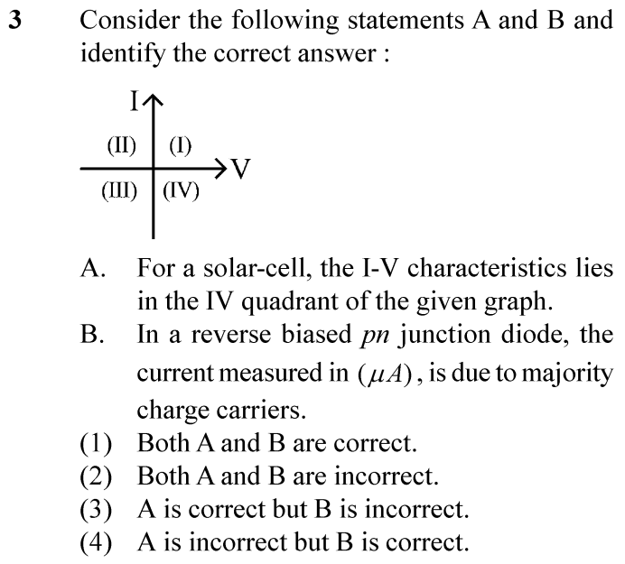
NEET 2024 · Q3 Easy
Official NEET 2024 Question 3 - Semiconductor Electronics: Materials, Devices and Simple Circuits
1
2
3 ✓ Key
4
💡 Verified Solution & 30-Second Hack
✓
Verified Against NTA Final Answer Key
Option (3) : A is correct but B is incorrect.
📚 Semiconductor Electronics Easy
📋 Given Parameters & Problem Setup
Statement A For a solar-cell, the I-V characteristics lies in the IV quadrant of the given graph.
Statement B In a reverse biased pn junction diode, the current measured in (μA), is due to majority charge carriers.
⚡

The 30-Second Exam Hall Shortcut: ⚡ Photocell & Reverse Bias 10-Second Recall

⏱️ Save ~40 seconds

Solar cell generates electrical power (delivers current at positive voltage -> IV quadrant); Reverse bias current is due to MINORITY carriers!

1 A solar cell does not consume power; it delivers power to a load, meaning when voltage is positive, current is drawn OUT of the cell (I < 0), placing its characteristic strictly in the 4th quadrant -> Statement A is CORRECT.
2 In reverse bias, the external field opposes majority carrier diffusion and sweeps MINORITY carriers across the junction, generating the tiny reverse saturation current in μA -> Statement B is INCORRECT.
3 Thus, A is correct but B is incorrect -> Pick Option (3) immediately!
🛡️
Why You Can 100% Trust This Shortcut: NCERT Physics · Semiconductor Electronics (Solar cell IV-characteristics and reverse bias minority carrier drift).
📐

Step-by-Step Rigorous Workflow & Mathematical Proof

Step 1

Analysis of Statement A (Solar Cell IV Characteristics)

A solar cell is a p-n junction diode operated without any external bias voltage. When sunlight illuminates the depletion region, electron-hole pairs are photogenerated. The internal junction electric field sweeps electrons to the n-side and holes to the p-side, setting up a photo-voltage. When connected across a load, it supplies current. Because it supplies power rather than drawing power, the current flows out of the positive terminal, resulting in a negative current convention for positive voltage. Hence, the I-V curve lies in the IV quadrant.

Pdelivered=V⋅I<0  ⟹  (V>0,I<0)∈Quadrant IVP_{delivered} = V \cdot I < 0 \implies (V > 0, I < 0) \in \text{Quadrant IV}
Step 2

Analysis of Statement B (Reverse Biased Diode Current)

When a p-n junction is reverse biased (p-side connected to negative terminal, n-side to positive terminal), the potential barrier height increases, completely blocking majority carriers from diffusing across the junction. The only current that flows is the reverse saturation current (order of microamperes, μA), which is caused solely by the drift of thermally generated MINORITY carriers (electrons from p-side and holes from n-side) swept across the depletion layer by the junction field. Therefore, the reverse current is due to minority carriers, not majority carriers.

Ireverse=I0∝density of minority carriersI_{reverse} = I_0 \propto \text{density of minority carriers}
Step 3

Verdict Synthesis

Statement A is completely correct. Statement B falsely claims the reverse current is due to majority carriers. Therefore, "A is correct but B is incorrect", matching Option (3).

Statement A: True,Statement B: False\text{Statement A: True}, \quad \text{Statement B: False}
⭐

360° Option Elimination Engine Key Feature

Diagnose every choice: Know exactly why the right option works and why distractors fail.

4-Option Deep Scan
1 (1)
✗ Incorrect
Verdict & Scientific Reason:

Incorrect because Statement B is false.

⚠️
Student Fallacy (Why candidates pick this trap): Believing that majority carriers flow in reverse bias.
2 (2)
✗ Incorrect
Verdict & Scientific Reason:

Incorrect because Statement A is true.

⚠️
Student Fallacy (Why candidates pick this trap): Thinking solar cells operate in the 1st quadrant like normal forward-biased LEDs.
3 (3)
✓ 100% Correct
Verdict & Scientific Reason:

Solar cell characteristics reside in the IV quadrant; reverse bias current is mediated by minority carriers.

💡
Why this is airtight: None; scientifically accurate.
4 (4)
✗ Incorrect
Verdict & Scientific Reason:

Completely inverted verdict for both statements.

⚠️
Student Fallacy (Why candidates pick this trap): Total misconception of both devices.
⚠️

NTA Trap Alert: Solar Cell vs Photodiode Operating Quadrants

Students confuse a photodiode (operated in 3rd quadrant under external reverse bias) with a solar cell (operated in 4th quadrant without external bias).

🛡️ How to avoid the -1 mark: Remember: Solar cells generate power without external bias -> Quadrant IV. Photodiodes detect light under reverse bias -> Quadrant III.
📖

Core NEET Syllabus Standard

Physics Core Modern Physics · Semiconductor Electronics: Materials, Devices and Simple Circuits Standard Benchmark
Core Scientific Principle Tested:

"Solar cells supply power and their I-V curve lies in the fourth quadrant; reverse saturation current in a p-n junction is governed entirely by minority carrier drift."

Syllabus Focus: p-n Junction Diode Applications and Solar Cells
✓ Core NEET UG Syllabus Anchor Syllabus & Academic Standards ↗
Solar Shines in Quadrant Four; Reverse Current is Minority Lore!
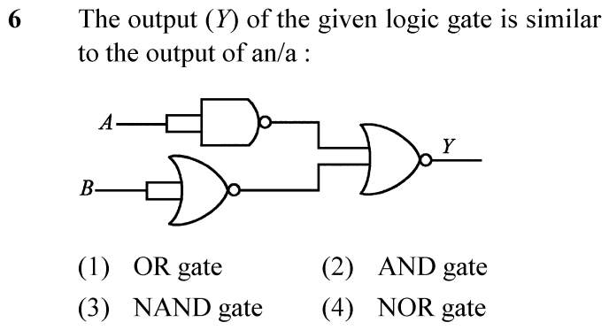
NEET 2024 · Q6 Easy
Official NEET 2024 Question 6 - Semiconductor Electronics: Materials, Devices and Simple Circuits
1
2 ✓ Key
3
4
💡 Verified Solution & 30-Second Hack
✓
Verified Against NTA Final Answer Key
Option (2) : AND gate
📚 Semiconductor Electronics Easy
📋 Given Parameters & Problem Setup
Input A Gate NAND gate with shorted inputs (acts as NOT gate)
Input B Gate NOR gate with shorted inputs (acts as NOT gate)
Output Gate NOR gate combining the inverted inputs
⚡

The 30-Second Exam Hall Shortcut: ⚡ De Morgan’s Inversion Shortcut

⏱️ Save ~40 seconds

Shorted NAND = NOT(A); Shorted NOR = NOT(B); Output NOR on (Ā, B̄) gives NOT(Ā + B̄) = A · B (AND Gate)!

1 A single-input NAND gate produces Ā (NOT A).
2 A single-input NOR gate produces B̄ (NOT B).
3 These feed into a NOR gate: Output Y = NOT(Ā + B̄).
4 By De Morgan’s First Theorem: NOT(Ā + B̄) = NOT(NOT A) · NOT(NOT B) = A · B.
5 The expression Y = A · B is the truth function of a standard AND gate -> Option (2) in 10 seconds!
🛡️
Why You Can 100% Trust This Shortcut: Boolean Algebra & De Morgan’s Theorems (NOT(A + B) = Ā · B̄).
📐

Step-by-Step Rigorous Workflow & Mathematical Proof

Step 1

Function of Input Gate for Terminal A

The top gate is a two-input NAND gate whose inputs are shorted together to receive a common signal A. The Boolean operation of a NAND gate on identical inputs simplifies directly to an inverter (NOT gate):

YA=A⋅A‾=A‾Y_A = \overline{A \cdot A} = \overline{A}
Step 2

Function of Input Gate for Terminal B

The bottom gate is a two-input NOR gate whose inputs are shorted together to receive a common signal B. The Boolean operation on identical inputs also simplifies to an inverter (NOT gate):

YB=B+B‾=B‾Y_B = \overline{B + B} = \overline{B}
Step 3

Final Stage NOR Gate Combination

The signals Y_A = Ā and Y_B = B̄ serve as inputs to the final NOR gate. The output Y is the NOR operation on Ā and B̄:

Y=YA+YB‾=A‾+B‾‾Y = \overline{Y_A + Y_B} = \overline{\overline{A} + \overline{B}}
Step 4

Simplification Using De Morgan’s Theorem

Applying De Morgan’s law to the complement of a sum yields the product of the complements:

Y=A‾‾⋅B‾‾=A⋅BY = \overline{\overline{A}} \cdot \overline{\overline{B}} = A \cdot B
⭐

360° Option Elimination Engine Key Feature

Diagnose every choice: Know exactly why the right option works and why distractors fail.

4-Option Deep Scan
1 (1)
✗ Incorrect
Verdict & Scientific Reason:

Represents A + B, whereas the circuit performs A · B.

⚠️
Student Fallacy (Why candidates pick this trap): Confusing De Morgan’s law and assuming the final NOR gate acts as an OR gate.
2 (2)
✓ 100% Correct
Verdict & Scientific Reason:

Boolean algebraic simplification proves Y = A · B identically.

💡
Why this is airtight: None.
3 (3)
✗ Incorrect
Verdict & Scientific Reason:

NAND would require an extra inversion at the output (NOT(A · B)).

⚠️
Student Fallacy (Why candidates pick this trap): Ignoring the inversion bubble of the final NOR gate.
4 (4)
✗ Incorrect
Verdict & Scientific Reason:

Only the final physical component is a NOR gate, but its inputs are already inverted.

⚠️
Student Fallacy (Why candidates pick this trap): Looking only at the final symbol without considering input inversions.
⚠️

NTA Trap Alert: Looking Only at the Final Gate

Hasty students look at the final gate symbol, see a NOR shape, and immediately circle NOR gate without checking the inverted inputs.

🛡️ How to avoid the -1 mark: Always write down the intermediate signals on your scratchpad: Y = NOT(Ā + B̄) = A · B.
📖

Core NEET Syllabus Standard

Physics Core Digital Electronics · Semiconductor Electronics: Materials, Devices and Simple Circuits Standard Benchmark
Core Scientific Principle Tested:

"Inverting both inputs to a NOR gate converts its functionality to that of an AND gate (bubbled NOR = AND)."

Syllabus Focus: Logic Gates and Universal Gate Combinations
✓ Core NEET UG Syllabus Anchor Syllabus & Academic Standards ↗
Inverted inputs flip the gate: NOR becomes AND, clear and straight!
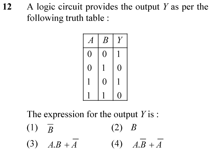
NEET 2024 · Q12 Easy
Official NEET 2024 Question 12 - Semiconductor Electronics: Materials, Devices and Simple Circuits
1 ✓ Key
2
3
4
💡 Verified Solution & 30-Second Hack
✓
Verified Against NTA Final Answer Key
Option (1) : B̄
📚 Semiconductor Electronics Easy
📋 Given Parameters & Problem Setup
Input A 0, 0, 1, 1
Input B 0, 1, 0, 1
Output Y 1, 0, 1, 0
⚡

The 30-Second Exam Hall Shortcut: ⚡ Independent Variable Inspection

⏱️ Save ~40 seconds

Notice Y is 1 when B=0, and Y is 0 when B=1 regardless of A -> Y = NOT(B) = B̄!

1 Inspect Row 1 and Row 3: When B = 0, Y = 1 (both for A=0 and A=1).
2 Inspect Row 2 and Row 4: When B = 1, Y = 0 (both for A=0 and A=1).
3 Output Y depends ONLY on input B, and is always the inverse of B.
4 Therefore, Y = B̄.
5 Option (1) in 3 seconds!
🛡️
Why You Can 100% Trust This Shortcut: Boolean Algebra Principles & Truth Table Analysis.
📐

Step-by-Step Rigorous Workflow & Mathematical Proof

Step 1

Tabulation and Pattern Analysis

Examine the given truth table row by row: - Row 1: A = 0, B = 0 -> Y = 1 - Row 2: A = 0, B = 1 -> Y = 0 - Row 3: A = 1, B = 0 -> Y = 1 - Row 4: A = 1, B = 1 -> Y = 0

Y(A,B)=B‾Y(A, B) = \overline{B}
Step 2

Sum-of-Products (SOP) Formulation

Writing the canonical minterms for the rows where the output Y is 1 (Row 1 and Row 3):

Y=A‾B‾+AB‾Y = \overline{A}\overline{B} + A\overline{B}
Step 3

Boolean Factoring and Simplification

Factor out the common term B̄ using the distributive law:

Y=B‾(A‾+A)=B‾(1)=B‾Y = \overline{B}(\overline{A} + A) = \overline{B}(1) = \overline{B}
⭐

360° Option Elimination Engine Key Feature

Diagnose every choice: Know exactly why the right option works and why distractors fail.

4-Option Deep Scan
1 (1)
✓ 100% Correct
Verdict & Scientific Reason:

Rigorous SOP Boolean reduction confirms Y = B̄.

💡
Why this is airtight: None.
2 (2)
✗ Incorrect
Verdict & Scientific Reason:

Inverts the output; when B=0, Y=1, not 0.

⚠️
Student Fallacy (Why candidates pick this trap): Assuming direct proportionality instead of inversion.
3 (3)
✗ Incorrect
Verdict & Scientific Reason:

For A=1, B=1, this expression gives 1 · 1 + 0 = 1, but truth table specifies Y=0.

⚠️
Student Fallacy (Why candidates pick this trap): Attempting algebraic expansion without verifying all truth table rows.
4 (4)
✗ Incorrect
Verdict & Scientific Reason:

For A=0, B=1, this expression gives 0 · 0 + 1 = 1, whereas the truth table gives Y=0.

⚠️
Student Fallacy (Why candidates pick this trap): Guessing multi-variable expressions.
⚠️

NTA Trap Alert: Over-Complicating with Both Variables

Students spend time setting up complex Karnaugh maps without noticing that A is a "don’t care" redundant variable.

🛡️ How to avoid the -1 mark: Always compare the output column directly against individual input columns first!
📖

Core NEET Syllabus Standard

Physics Core Digital Electronics · Semiconductor Electronics: Materials, Devices and Simple Circuits Standard Benchmark
Core Scientific Principle Tested:

"When an output is high whenever a specific input is low and vice-versa regardless of other inputs, the function reduces to the single-variable NOT operation (Y = X̄)."

Syllabus Focus: Boolean Algebra and Logic Functions
✓ Core NEET UG Syllabus Anchor Syllabus & Academic Standards ↗
A changes but Y ignores; Y is NOT B and nothing more!
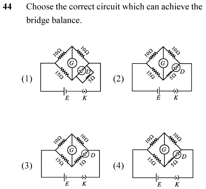
NEET 2024 · Q44 Medium
Official NEET 2024 Question 44 - Semiconductor Electronics: Materials, Devices and Simple Circuits
1
2
3 ✓ Key
4
💡 Verified Solution & 30-Second Hack
✓
Verified Against NTA Final Answer Key
Option (3) : Circuit (3) with forward-biased diode in series with 5 Ω resistor
📚 Semiconductor Electronics Medium
📋 Given Parameters & Problem Setup
Bridge configuration Wheatstone bridge with battery E having positive terminal on left
Top arms 10 Ω (top-left) and 10 Ω (top-right)
Bottom-left arm 15 Ω
Bottom-right arm Diode D in series/parallel with 5 Ω resistor
⚡

The 30-Second Exam Hall Shortcut: ⚡ Forward-Bias Diode Conduction Rule

⏱️ Save ~40 seconds

For bridge balance, current must flow normally through all arms -> Diode must be FORWARD BIASED in series -> Circuit (3) has diode anode pointing from bottom node to right node!

1 A Wheatstone bridge requires current to establish steady potentials at the galvanometer nodes.
2 Battery positive terminal is on the left: current enters the left junction and flows towards the right junction (negative terminal).
3 In the lower branch, current must flow from the bottom node towards the right junction.
4 For a diode to conduct in this branch, it MUST be forward biased: its anode (triangle) must point towards the cathode (bar) in the direction of current flow (from bottom to right).
5 In Circuit (4), the diode is pointing backward (reverse biased) -> blocks current completely.
6 In Circuit (1) and (2), parallel configurations cannot achieve balance.
7 Circuit (3) correctly forward-biases the series diode, enabling balance -> Option (3)!
🛡️
Why You Can 100% Trust This Shortcut: p-n Junction Diode Unidirectional Conduction & Bridge Balance Principles.
📐

Step-by-Step Rigorous Workflow & Mathematical Proof

Step 1

Principle of Wheatstone Bridge Balance

For a bridge to achieve balance, the potential difference across the galvanometer G must be zero (V_top = V_bottom), which requires continuous current flow through all four resistive branches establishing a stable potential divider.

Vtop=Vbottom  ⟹  IG=0V_{top} = V_{bottom} \implies I_G = 0
Step 2

Direction of Potential Gradient and Current Flow

The DC source E is connected with its positive terminal on the left and negative terminal on the right. Current enters at the left node, divides into the upper and lower arms, and exits at the right node. In the bottom-right arm, the conventional current MUST flow from the lower central junction towards the right-hand junction connected to the negative terminal of the battery.

Vbottom node>Vright node  ⟹  Current flows bottom→rightV_{bottom\,node} > V_{right\,node} \implies \text{Current flows bottom} \rightarrow \text{right}
Step 3

Diode Biasing Requirement

A p-n junction diode conducts current only when it is forward biased (p-side/anode at higher potential than n-side/cathode). In Circuit (3), the anode is connected to the bottom junction and cathode to the right junction, so it is forward biased and conducts freely. In Circuit (4), the diode is reverse biased, presenting near-infinite resistance and preventing current flow.

Forward Bias: Anode (+)→Cathode (−)\text{Forward Bias: Anode } (+) \rightarrow \text{Cathode } (-)
Step 4

Selection of Circuit (3)

Therefore, only Circuit (3) allows proper forward-biased conduction through the diode in series with the 5 Ω resistor, making it the only circuit that can establish the required currents and achieve bridge balance.

Circuit (3) achieves bridge balance\text{Circuit (3) achieves bridge balance}
⭐

360° Option Elimination Engine Key Feature

Diagnose every choice: Know exactly why the right option works and why distractors fail.

4-Option Deep Scan
1 (1)
✗ Incorrect
Verdict & Scientific Reason:

Parallel diode clamps voltage and prevents linear bridge balance.

⚠️
Student Fallacy (Why candidates pick this trap): Assuming parallel bypass diode can balance the arm.
2 (2)
✗ Incorrect
Verdict & Scientific Reason:

Cannot achieve balance.

⚠️
Student Fallacy (Why candidates pick this trap): Misinterpreting diode behavior.
3 (3)
✓ 100% Correct
Verdict & Scientific Reason:

Diode is properly forward-biased in the direction of conventional current flow.

💡
Why this is airtight: None.
4 (4)
✗ Incorrect
Verdict & Scientific Reason:

Diode is reverse biased and acts as an open circuit (I = 0).

⚠️
Student Fallacy (Why candidates pick this trap): Overlooking diode polarity.
⚠️

NTA Trap Alert: Ignoring Diode Arrow Direction

Students look at the resistor values and treat the diode as a plain wire, failing to check whether the diode arrow points with or against the battery current.

🛡️ How to avoid the -1 mark: Trace current from battery (+) to (-). The diode triangle MUST point in the direction the current wants to go!
📖

Core NEET Syllabus Standard

Physics Core Electronics · Semiconductor Electronics: Materials, Devices and Simple Circuits Standard Benchmark
Core Scientific Principle Tested:

"A p-n junction diode conducts when forward-biased and acts as an open circuit when reverse-biased; bridge balance requires all arms to conduct."

Syllabus Focus: p-n Junction Diode as a Circuit Element
✓ Core NEET UG Syllabus Anchor Syllabus & Academic Standards ↗
Follow the current from left to right: Diode must point in the arrow’s light (Circuit 3)!
NEET 2023 · Q13 Easy
Official NEET 2023 Question 13 - Semiconductor Electronics: Materials, Devices and Simple Circuits
1
2 ✓ Key
3
4
💡 Verified Solution & 30-Second Hack
✓
Verified Against NTA Final Answer Key
Option (2) : Both Statement I and Statement II are correct.
📚 Semiconductor Electronics: Materials, Devices and Simple Circuits Easy
📋 Given Parameters & Problem Setup
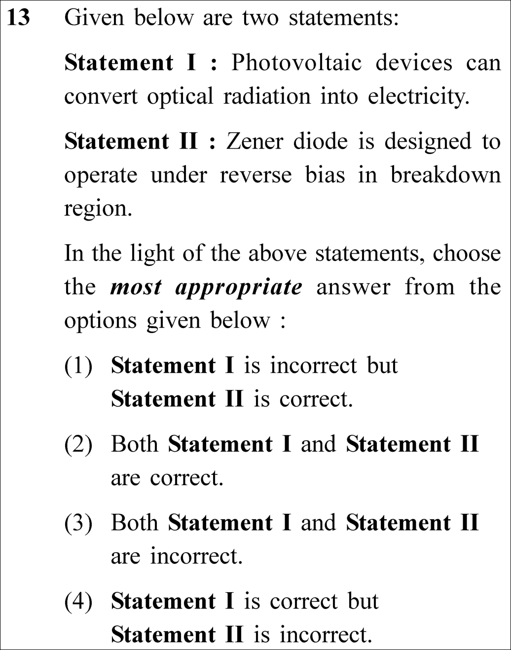
Statement I Photovoltaic devices can convert optical radiation into electricity.
Statement II Zener diode is designed to operate under reverse bias in breakdown region.
⚡

The 30-Second Exam Hall Shortcut: ⚡ NCERT Direct Conceptual Verification

⏱️ Save ~40 seconds

Photovoltaic = Photo (light) to Volt (electricity); Zener diode = Reverse breakdown voltage regulator. Both are verbatim true statements!

1 Inspect Statement I: Solar cells / photovoltaic cells absorb photons to generate electron-hole pairs, converting optical radiation into electrical power. This is strictly TRUE.
2 Inspect Statement II: Zener diodes are heavily doped p-n junctions engineered specifically to operate safely in the reverse breakdown zone without damage. This is strictly TRUE.
3 Conclude immediately that both statements are correct.
4 Pick Option (2) in 5 seconds flat!
🛡️
Why You Can 100% Trust This Shortcut: NCERT Physics · Semiconductor Electronics (Photovoltaic generation: optical to electrical conversion; Zener diode operating point: reverse breakdown region).
📐

Step-by-Step Rigorous Workflow & Mathematical Proof

Step 1

Validation of Statement I (Photovoltaic Devices)

A photovoltaic device (solar cell) operates on the principle of the photovoltaic effect. When incident photons of energy hν > E_g strike the junction, electron-hole pairs are generated in the depletion region. The built-in junction electric field separates electrons to the n-side and holes to the p-side, establishing a photo-voltage across an external load without any external bias:

hν≥Eg  ⟹  Optical Radiation⟶Electrical Energyh\nu \ge E_g \implies \text{Optical Radiation} \longrightarrow \text{Electrical Energy}
Step 2

Validation of Statement II (Zener Diode Operation)

A Zener diode is a special-purpose semiconductor diode that is heavily doped on both p and n sides, resulting in a very thin depletion layer (~10⁻⁶ m) and intense junction electric field (~5 × 10⁶ V/m). It is specifically designed to operate under reverse bias in the Zener breakdown region, where the voltage across it remains virtually constant despite sharp variations in current, serving as a voltage stabilizer:

Vreverse=VZ=constant(in reverse breakdown region)V_{\text{reverse}} = V_Z = \text{constant} \quad (\text{in reverse breakdown region})
Step 3

Final Combined Deduction

Since both Statement I and Statement II represent foundational, canonical principles of semiconductor devices, Option (2) is the uniquely correct choice.

⭐

360° Option Elimination Engine Key Feature

Diagnose every choice: Know exactly why the right option works and why distractors fail.

4-Option Deep Scan
1 (1)
✗ Incorrect
Verdict & Scientific Reason:

Falsely declares photovoltaic devices do not convert light to electricity.

⚠️
Student Fallacy (Why candidates pick this trap): Candidate confused photovoltaic with photoconductive or LED devices.
2 (2)
✓ 100% Correct
Verdict & Scientific Reason:

Both statements are factually and theoretically accurate according to standard semiconductor physics.

💡
Why this is airtight: None. Candidate correctly verified both optoelectronic and breakdown principles.
3 (3)
✗ Incorrect
Verdict & Scientific Reason:

Both statements are canonical textbook truths.

⚠️
Student Fallacy (Why candidates pick this trap): Candidate incorrectly thought Zener diodes operate in forward bias.
4 (4)
✗ Incorrect
Verdict & Scientific Reason:

Falsely asserts Zener diode does not operate in reverse breakdown.

⚠️
Student Fallacy (Why candidates pick this trap): Candidate confused general rectifier diodes (which avoid breakdown) with Zener diodes (which are built for breakdown).
⚠️

NTA Trap Alert: Confusing Standard Diode Breakdown with Zener Diode Design

In normal rectifier diodes, reverse breakdown can cause thermal runaway and destroy the device. In Zener diodes, heavy doping allows safe, reversible, continuous operation in reverse breakdown.

🛡️ How to avoid the -1 mark: Remember: Zener diodes are uniquely manufactured TO OPERATE in reverse breakdown as voltage regulators.
📖

Core NEET Syllabus Standard

National Eligibility cum Entrance Test (NEET UG) · Semiconductor Electronics: Materials, Devices and Simple Circuits Standard Benchmark
Core Scientific Principle Tested:

"Solar cells generate EMF from optical radiation; Zener diodes maintain stable voltage in reverse breakdown."

Syllabus Focus: Special Purpose p-n Junction Diodes: Solar Cells and Zener Diode
Preserved in Rationalized Curriculum Syllabus & Academic Standards ↗
NEET 2023 · Q20 Easy
Official NEET 2023 Question 20 - Semiconductor Electronics: Materials, Devices and Simple Circuits
1
2
3
4 ✓ Key
💡 Verified Solution & 30-Second Hack
✓
Verified Against NTA Final Answer Key
Option (4) : Capacitor
📚 Semiconductor Electronics: Materials, Devices and Simple Circuits Easy
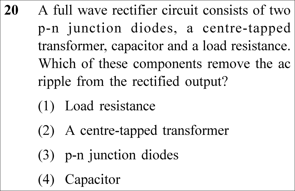
📋 Given Parameters & Problem Setup
Circuit Full wave rectifier with centre-tapped transformer, 2 diodes, capacitor, and load resistor
Target Action Component that removes the AC ripple from rectified output
⚡

The 30-Second Exam Hall Shortcut: ⚡ Filter Circuit Component Memory Hook

⏱️ Save ~30 seconds

A rectifier converts AC to pulsating DC; to smooth/remove the AC ripple, a CAPACITOR filter (or inductor choke) is used!

1 Diodes perform rectification (convert bidirectional AC into pulsating unidirectional DC).
2 The output across the diodes contains both a DC component and an unwanted AC ripple.
3 To remove/filter this AC ripple, a capacitor is connected in parallel with the load (or an inductor in series).
4 The capacitor offers low reactance to AC (X_C = 1/ωC) bypassing it to ground, while blocking DC and forcing steady DC through the load.
5 Therefore, the Capacitor removes the AC ripple. Instant Option (4)!
🛡️
Why You Can 100% Trust This Shortcut: NCERT Physics · Semiconductor Electronics (Filter circuits: Capacitor connected in parallel with load resistance removes the AC ripple).
📐

Step-by-Step Rigorous Workflow & Mathematical Proof

Step 1

Nature of Rectified Output

The output of a full-wave rectifier consisting of two p-n junction diodes and a center-tapped transformer is unidirectional but pulsates periodically with twice the input frequency (ripple frequency = 2f). This output consists of a desired DC component superimposed with unwanted AC ripple harmonics.

Step 2

Role of Capacitor as a Filter

To obtain a steady DC voltage without fluctuations, a filter circuit is employed. A capacitor filter is connected in parallel with the load resistance R_L. Its capacitive reactance is frequency-dependent:

XC=12πfrippleCX_C = \frac{1}{2\pi f_{\text{ripple}} C}
Step 3

Bypass Mechanism

For the high-frequency AC ripple components, X_C is very low, providing an easy low-impedance bypass path. For DC (f = 0), X_C → ∞, meaning zero DC current leaks through the capacitor, forcing steady DC voltage across the load resistance R_L:

XC,DC=∞,XC,AC≪RLX_{C,\text{DC}} = \infty, \qquad X_{C,\text{AC}} \ll R_L
⭐

360° Option Elimination Engine Key Feature

Diagnose every choice: Know exactly why the right option works and why distractors fail.

4-Option Deep Scan
1 (1)
✗ Incorrect
Verdict & Scientific Reason:

The load resistance consumes output power and dissipates current; it has no filtering capability.

⚠️
Student Fallacy (Why candidates pick this trap): Candidate confused the output load terminal with the filtering element.
2 (2)
✗ Incorrect
Verdict & Scientific Reason:

The transformer steps down AC voltage and provides out-of-phase AC signals for alternating conduction.

⚠️
Student Fallacy (Why candidates pick this trap): Candidate confused voltage transformation with ripple suppression.
3 (3)
✗ Incorrect
Verdict & Scientific Reason:

Diodes perform rectification (converting AC into pulsating DC); they create the ripple, not filter it.

⚠️
Student Fallacy (Why candidates pick this trap): Candidate confused the rectification stage with the filtering stage.
4 (4)
✓ 100% Correct
Verdict & Scientific Reason:

Accurate component: capacitor acts as a low-pass filter, smoothing pulsating voltage and removing AC ripple.

💡
Why this is airtight: None. Candidate correctly identified the capacitor filter circuit.
⚠️

NTA Trap Alert: Confusing Rectification (Diodes) with Filtering (Capacitor)

Many candidates see "remove AC" and think of the diodes. Diodes remove the negative half-cycles to make current unidirectional, but the capacitor removes the ripple to make it smooth DC.

🛡️ How to avoid the -1 mark: Diodes = Rectifier. Capacitor = Filter (Ripple Remover).
📖

Core NEET Syllabus Standard

National Eligibility cum Entrance Test (NEET UG) · Semiconductor Electronics: Materials, Devices and Simple Circuits Standard Benchmark
Core Scientific Principle Tested:

"Capacitor connected in parallel across load resistance charges during peak voltage and discharges through load during dips, removing AC ripple."

Syllabus Focus: Full Wave Rectifier and Capacitor Filter Circuits
Preserved in Rationalized Curriculum Syllabus & Academic Standards ↗
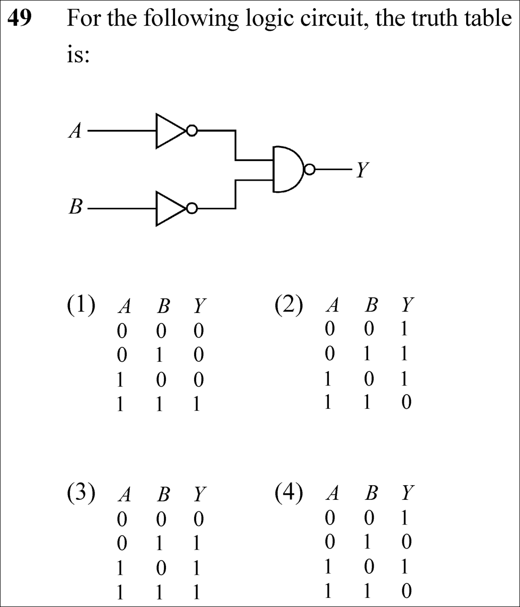
NEET 2023 · Q49 Easy
Official NEET 2023 Question 49 - Semiconductor Electronics: Materials, Devices and Simple Circuits
1
2
3 ✓ Key
4
💡 Verified Solution & 30-Second Hack
✓
Verified Against NTA Final Answer Key
Option (3) : OR Gate Truth Table (0,0→0; 0,1→1; 1,0→1; 1,1→1)
📚 Semiconductor Electronics: Materials, Devices and Simple Circuits Easy
📋 Given Parameters & Problem Setup
Inputs A, B
Input stage NOT gates giving Ā and B̄
Output stage NAND gate receiving Ā and B̄
Boolean Expression Y = (Ā · B̄)̄ = A + B
⚡

The 30-Second Exam Hall Shortcut: ⚡ De Morgan’s Inversion Hack: (Ā · B̄)̄ = A + B

⏱️ Save ~40 seconds

Bubble-NAND is an OR gate! Inputs inverted before NAND: Y = (Ā · B̄)̄ = A + B. This is an OR gate truth table (outputs 1 if ANY input is 1) in 5 seconds!

1 Trace the circuit: Input A passes through a NOT gate to become Ā.
2 Input B passes through a NOT gate to become B̄.
3 Both inverted signals feed into a NAND gate.
4 Output equation: Y = (Ā · B̄)̄.
5 Apply De Morgan’s First Theorem: (X · Z)̄ = X̄ + Z̄ ⟹ (Ā · B̄)̄ = A̿ + B̿ = A + B.
6 The entire combination is an OR gate! Its truth table outputs 0 only for (0,0), and 1 for all other inputs.
7 Select Option (3) OR Gate truth table!
🛡️
Why You Can 100% Trust This Shortcut: Digital Electronics · Boolean Algebra & De Morgan’s Laws ((Ā · B̄)̄ = A + B represents the universal NAND gate realization of an OR gate).
📐

Step-by-Step Rigorous Workflow & Mathematical Proof

Step 1

Circuit Schematic Analysis

The given digital logic circuit contains two NOT gates (inverters) connected to inputs A and B, respectively. The outputs of these two inverters, Ā and B̄, serve as the inputs to a two-input NAND gate.

Inverter Outputs: Aˉ,Bˉ\text{Inverter Outputs: } \bar{A}, \quad \bar{B}
Step 2

Formulation of Boolean Expression

A NAND gate performs an AND operation followed by a negation. Therefore, the output Y is expressed as:

Y=Aˉ⋅Bˉ‾Y = \overline{\bar{A} \cdot \bar{B}}
Step 3

Application of De Morgan’s Theorem

By De Morgan’s second theorem of Boolean algebra, the complement of a product of variables equals the sum of their individual complements:

X⋅Z‾=Xˉ+Zˉ  ⟹  Y=Aˉ‾+Bˉ‾=A+B\overline{X \cdot Z} = \bar{X} + \bar{Z} \implies Y = \overline{\bar{A}} + \overline{\bar{B}} = A + B
Step 4

Construction of the Resultant Truth Table

The expression Y = A + B corresponds identically to a standard OR gate:

ABAˉBˉAˉ⋅BˉY=Aˉ⋅Bˉ‾=A+B001110011001100101110001\begin{array}{|c|c|c|c|c|c|} \hline A & B & \bar{A} & \bar{B} & \bar{A} \cdot \bar{B} & Y = \overline{\bar{A} \cdot \bar{B}} = A + B \\ \hline 0 & 0 & 1 & 1 & 1 & 0 \\ 0 & 1 & 1 & 0 & 0 & 1 \\ 1 & 0 & 0 & 1 & 0 & 1 \\ 1 & 1 & 0 & 0 & 0 & 1 \\ \hline \end{array}
⭐

360° Option Elimination Engine Key Feature

Diagnose every choice: Know exactly why the right option works and why distractors fail.

4-Option Deep Scan
1 (1)
✗ Incorrect
Verdict & Scientific Reason:

Truth table of an AND gate (Y = A · B).

⚠️
Student Fallacy (Why candidates pick this trap): Candidate forgot the inversion bubble on the NAND gate.
2 (2)
✗ Incorrect
Verdict & Scientific Reason:

Truth table of a standard NAND gate without inverted inputs.

⚠️
Student Fallacy (Why candidates pick this trap): Candidate ignored the two input inverters.
3 (3)
✓ 100% Correct
Verdict & Scientific Reason:

Accurate truth table of an OR gate: Y = A + B.

💡
Why this is airtight: None. Candidate correctly applied De Morgan’s law.
4 (4)
✗ Incorrect
Verdict & Scientific Reason:

Inverted parity table.

⚠️
Student Fallacy (Why candidates pick this trap): Candidate made logic errors during individual truth evaluations.
⚠️

NTA Trap Alert: Confusing Negative-Input NAND (OR Gate) with Negative-Input AND (NOR Gate)

Feeding inverted inputs into a NAND gate yields (Ā · B̄)̄ = A + B (an OR gate). Feeding inverted inputs into an AND gate yields Ā · B̄ = (A + B)̄ (a NOR gate). Keeping track of the bubble on the NAND gate prevents this confusion.

🛡️ How to avoid the -1 mark: Use De Morgan duality: "Bubble at inputs + Bubble at output" of an AND gate transforms it into a standard OR gate!
📖

Core NEET Syllabus Standard

National Eligibility cum Entrance Test (NEET UG) · Semiconductor Electronics: Materials, Devices and Simple Circuits Standard Benchmark
Core Scientific Principle Tested:

"By De Morgan’s laws, (Ā · B̄)̄ = A + B, which realizes the OR logic function."

Syllabus Focus: Logic Gates and Universal Gate Combinations
Preserved in Rationalized Curriculum Syllabus & Academic Standards ↗
NEET 2021 · Q13 Easy
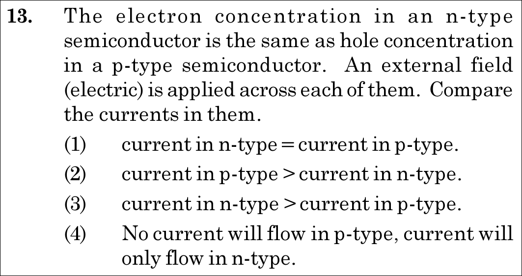
Official NEET 2021 Question 13 - Semiconductor Electronics: Materials, Devices and Simple Circuits
1
2
3 ✓ Key
4
💡 Verified Solution & 30-Second Hack
✓
Verified Against NTA Final Answer Key
Option (3) : current in n-type > current in p-type.
📚 Semiconductor Electronics: Materials, Devices and Simple Circuits Easy
📋 Given Parameters & Problem Setup
Electron concentration in n-type (n_e) Equal to hole concentration in p-type (n_h)
External Electric Field (E) Same for both
⚡

The 30-Second Exam Hall Shortcut: ⚡ Electron Mobility Rule: μ_e > μ_h   ⟹  \implies I_n > I_p

⏱️ Save ~20 seconds

Electrons move freely in the conduction band, whereas holes move through valence bond step-by-step jumping. Hence, electron mobility is always strictly greater than hole mobility (μe>μh\mu_e > \mu_h). With identical carrier densities and electric fields, In>IpI_n > I_p! Match Option (3)!

1 Current in semiconductor: I=nqAvd=nqAμEI = n q A v_d = n q A \mu E.
2 For n-type: In=neeAμeEI_n = n_e e A \mu_e E. For p-type: Ip=nheAμhEI_p = n_h e A \mu_h E.
3 Given ne=nhn_e = n_h and EE is identical.
4 Since electrons in conduction band have higher mobility than valence band holes (μe>μh\mu_e > \mu_h), we have In>IpI_n > I_p.
5 Match Option (3) current in n-type > current in p-type.
🛡️
Why You Can 100% Trust This Shortcut: Canonical solid state physics energy band theory of carrier mobility.
📐

Step-by-Step Rigorous Workflow & Mathematical Proof

Step 1

Formulating Current in Terms of Carrier Mobility

The drift velocity of a charge carrier under an electric field EE is vd=μEv_d = \mu E, where μ\mu is mobility. Current through a semiconductor of cross-sectional area AA with carrier concentration nn is:

I=neAvd=neAμEI = n e A v_d = n e A \mu E
Step 2

Comparing n-type and p-type Currents

For n-type with electron density nen_e and p-type with hole density nhn_h:

In=neeAμeE,Ip=nheAμhEI_n = n_e e A \mu_e E, \quad I_p = n_h e A \mu_h E
Step 3

Physical Reason for Mobility Difference

Electrons in n-type occupy the conduction band, where they behave almost as free electrons with small effective mass. Holes in p-type move via the sequential vacancy-hopping of bound valence electrons. Consequently, in all semiconductors (Silicon, Germanium, GaAs):

μe>μh  ⟹  In>Ip\mu_e > \mu_h \implies I_n > I_p
⭐

360° Option Elimination Engine Key Feature

Diagnose every choice: Know exactly why the right option works and why distractors fail.

4-Option Deep Scan
1 1
✗ Incorrect
Verdict & Scientific Reason:

Fails to consider that electrons and holes have different mobilities ($mu_e eq mu_h$).

⚠️
Student Fallacy (Why candidates pick this trap): Assuming equal carrier concentrations guarantee equal currents.
2 2
✗ Incorrect
Verdict & Scientific Reason:

Inverts the mobility relationship (holes never have higher mobility than electrons).

⚠️
Student Fallacy (Why candidates pick this trap): Falsely assuming holes move faster.
3 3
✓ 100% Correct
Verdict & Scientific Reason:

Exact physical conclusion: because mue>muhmu_e > mu_h, the drift current in n-type exceeds that in p-type.

💡
Why this is airtight: None; rigorous semiconductor physics.
4 4
✗ Incorrect
Verdict & Scientific Reason:

Holes are mobile positive charge carriers that conduct macroscopic current readily.

⚠️
Student Fallacy (Why candidates pick this trap): Thinking holes cannot conduct electrical current.
⚠️

NTA Trap Alert: Carrier Density vs. Current Equality Trap

Students frequently equate current solely with carrier density (I∝nI \propto n), forgetting that current also depends on drift velocity (vd=μEv_d = \mu E). Since μe>μh\mu_e > \mu_h, current in n-type is always greater.

🛡️ How to avoid the -1 mark: Remember: I=neAμEI = n e A \mu E. Even if ne=nhn_e = n_h, electron mobility is ALWAYS higher (μe>μh\mu_e > \mu_h).
📖

Core NEET Syllabus Standard

NCERT Physics · Semiconductor Electronics: Materials, Devices and Simple Circuits Standard Benchmark
Core Scientific Principle Tested:

"Electron mobility in conduction band is significantly higher than hole mobility in valence band (μe>μh\mu_e > \mu_h)."

Syllabus Focus: Extrinsic Semiconductors
✓ Core NEET UG Syllabus Anchor Syllabus & Academic Standards ↗
NEET 2021 · Q23 Easy
Official NEET 2021 Question 23 - Semiconductor Electronics: Materials, Devices and Simple Circuits
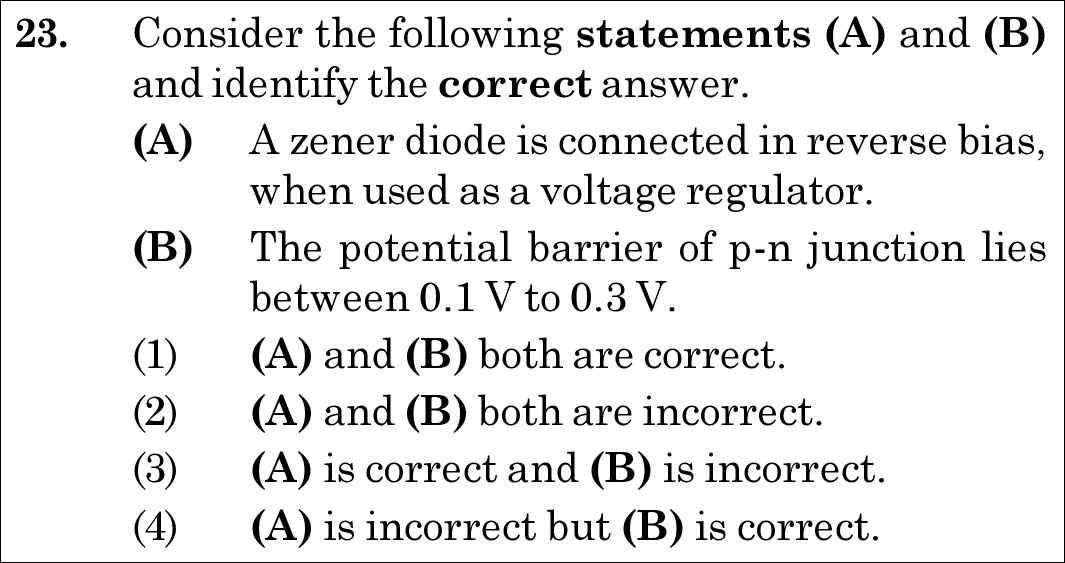
1 (A) and (B) both are correct.
2 (A) and (B) both are incorrect.
3 (A) is correct and (B) is incorrect. ✓ Key
4 (A) is incorrect but (B) is correct.
💡 Verified Solution & 30-Second Hack
✓
Verified Against NTA Final Answer Key
Option (3) : (A) is correct and (B) is incorrect.
📚 Semiconductor Electronics: Materials, Devices and Simple Circuits Easy
📋 Given Parameters & Problem Setup
Statement (A) A zener diode is connected in reverse bias, when used as a voltage regulator.
Statement (B) The potential barrier of p-n junction lies between 0.1 V to 0.3 V.
⚡

The 30-Second Exam Hall Shortcut: ⚡ Zener Reverse Bias + Silicon 0.7 V Barrier Rule

⏱️ Save ~20 seconds

Statement (A) is TRUE: Zener diode operates strictly in reverse-breakdown region for voltage regulation. Statement (B) is FALSE: Silicon p-n junctions have a barrier potential of ≈0.7 V\approx 0.7\text{ V} (Germanium is ≈0.3 V\approx 0.3\text{ V}), so the barrier lies typically between 0.3 V0.3\text{ V} and 0.7 V0.7\text{ V}, not 0.1 V0.1\text{ V} to 0.3 V0.3\text{ V}! Match Option (3)!

1 Check Statement (A): Voltage regulator operation requires reverse bias in breakdown region -> True.
2 Check Statement (B): Claims barrier potential is 0.1 V to 0.3 V. But standard Si barrier is ~0.7 V and Ge is ~0.3 V -> False.
3 Thus, (A) is correct and (B) is incorrect.
4 Match Option (3).
🛡️
Why You Can 100% Trust This Shortcut: Canonical NCERT Semiconductor Electronics semiconductor device fundamentals.
📐

Step-by-Step Rigorous Workflow & Mathematical Proof

Step 1

Evaluation of Statement (A): Zener Diode Operation

A Zener diode is a heavily doped silicon p-n junction diode. When operated in the reverse breakdown region, the voltage across the diode (VZV_Z) remains virtually constant over a wide range of reverse currents (IZI_Z). Therefore, to regulate unregulated DC voltage, it is always connected in reverse bias across the load:

Zener Voltage Regulator  ⟹  Operates in Reverse Breakdown Bias (Statement A is CORRECT)\text{Zener Voltage Regulator} \implies \mathbf{\text{Operates in Reverse Breakdown Bias (Statement A is CORRECT)}}
Step 2

Evaluation of Statement (B): p-n Junction Barrier Potential

In an unbiased p-n junction, diffusion of majority carriers creates a depletion layer with a built-in potential barrier V0V_0. For Germanium, V0≈0.3 VV_0 \approx 0.3\text{ V}, and for Silicon (the ubiquitous material in modern electronics), V0≈0.7 VV_0 \approx 0.7\text{ V}. Thus, the barrier potential typically lies between 0.3 V0.3\text{ V} and 0.7 V0.7\text{ V}, not between 0.1 V0.1\text{ V} and 0.3 V0.3\text{ V}. Statement (B) is unambiguously incorrect.

Step 3

Conclusion

Statement (A) is correct and Statement (B) is incorrect. This corresponds uniquely to Option (3).

⭐

360° Option Elimination Engine Key Feature

Diagnose every choice: Know exactly why the right option works and why distractors fail.

4-Option Deep Scan
1 1
✗ Incorrect
Verdict & Scientific Reason:

Statement (B) is false because Silicon p-n junctions have a barrier potential of ~0.7 V.

⚠️
Student Fallacy (Why candidates pick this trap): Believing 0.1 V to 0.3 V covers all semiconductor junctions.
2 2
✗ Incorrect
Verdict & Scientific Reason:

Statement (A) is an undisputed textbook fact of semiconductor electronics.

⚠️
Student Fallacy (Why candidates pick this trap): Doubting whether Zener diodes operate in reverse bias.
3 3
✓ 100% Correct
Verdict & Scientific Reason:

Statement (A) accurately states reverse-bias operation of Zener regulators, while Statement (B) underestimates the barrier potential range.

💡
Why this is airtight: None; rigorous semiconductor physics knowledge.
4 4
✗ Incorrect
Verdict & Scientific Reason:

Inverts the truth value of both statements.

⚠️
Student Fallacy (Why candidates pick this trap): Gross confusion regarding semiconductor diode physics.
⚠️

NTA Trap Alert: Germanium vs. Silicon Barrier Potential Trap

Students often recall that Germanium has a low barrier potential of ≈0.3 V\approx 0.3\text{ V} and assume Statement (B) is true, forgetting that Silicon (the primary semiconductor in NCERT) has a barrier of ≈0.7 V\approx 0.7\text{ V}.

🛡️ How to avoid the -1 mark: Remember: Silicon barrier potential is ≈0.7 V\approx 0.7\text{ V}. Any range ending at 0.3 V0.3\text{ V} is false for p-n junctions.
📖

Core NEET Syllabus Standard

NCERT Physics · Semiconductor Electronics: Materials, Devices and Simple Circuits Standard Benchmark
Core Scientific Principle Tested:

"A Zener diode is designed to operate continuously in the reverse breakdown region as a voltage regulator. The barrier potential of a silicon p-n junction is approximately 0.7 V."

Syllabus Focus: p-n Junction Diode and Zener Diode
✓ Core NEET UG Syllabus Anchor Syllabus & Academic Standards ↗
NEET 2021 · Q39 Medium
Official NEET 2021 Question 39 - Semiconductor Electronics: Materials, Devices and Simple Circuits
1
2
3 ✓ Key
4
💡 Verified Solution & 30-Second Hack
✓
Verified Against NTA Final Answer Key
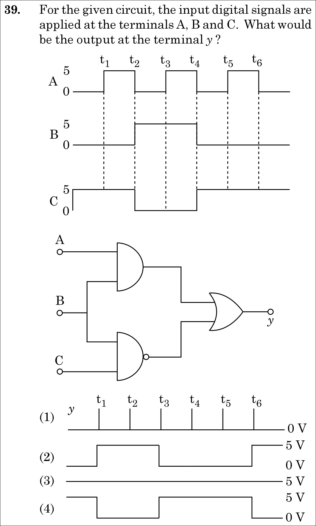
Option (3) : Graph (3): Constant high output at 5 V across all time intervals
📚 Semiconductor Electronics: Materials, Devices and Simple Circuits Medium
📋 Given Parameters & Problem Setup
Gate 1 (Top) AND gate with inputs A and B (Output = A · B)
Gate 2 (Bottom) NAND gate with inputs B and C (Output = (B · C)')
Gate 3 (Output) OR gate receiving outputs of Gate 1 and Gate 2 (y = (A · B) + (B · C)')
⚡

The 30-Second Exam Hall Shortcut: ⚡ NAND Gate is ALWAYS 1 because B and C are NEVER simultaneously 1!

⏱️ Save ~30 seconds

Inspect the waveform: When B=1B = 1 (5 V5\text{ V}, between t2t_2 and t4t_4), CC is strictly 00! When C=1C = 1, BB is strictly 00! Thus, BB and CC are NEVER simultaneously 1   ⟹  B⋅C=0\implies B \cdot C = 0 at all times! Therefore, the NAND gate output B⋅C‾=1\overline{B \cdot C} = 1 (5 V5\text{ V}) permanently! Since an OR gate with a constant 1 input outputs 1, y=5 Vy = 5\text{ V} constantly! Match Graph (3)!

1 Boolean expression: y=(A⋅B)+B⋅C‾y = (A \cdot B) + \overline{B \cdot C}.
2 Examine inputs B and C in the timing diagram: - Before t2t_2: B=0,C=1  ⟹  B⋅C=0B = 0, C = 1 \implies B \cdot C = 0. - t2t_2 to t4t_4: B=1,C=0  ⟹  B⋅C=0B = 1, C = 0 \implies B \cdot C = 0. - After t4t_4: B=0,C=1  ⟹  B⋅C=0B = 0, C = 1 \implies B \cdot C = 0.
3 At every instant of time, B⋅C=0B \cdot C = 0.
4 Therefore, the output of the NAND gate is B⋅C‾=0‾=1\overline{B \cdot C} = \overline{0} = 1 (5 V5\text{ V}) continuously.
5 The OR gate output is y=(A⋅B)+1=1y = (A \cdot B) + 1 = 1 (5 V5\text{ V}) continuously across all intervals.
6 Match Graph (3).
🛡️
Why You Can 100% Trust This Shortcut: Canonical Boolean algebra identities (X+1=1X + 1 = 1) and digital waveform timing analysis.
📐

Step-by-Step Rigorous Workflow & Mathematical Proof

Step 1

Formulating the Output Boolean Function

Analyze the logic gate circuit: - Gate 1 is an AND gate with inputs AA and BB, giving output Y1=A⋅BY_1 = A \cdot B. - Gate 2 is a NAND gate with inputs BB and CC, giving output Y2=B⋅C‾Y_2 = \overline{B \cdot C}. - Gate 3 is an OR gate combining Y1Y_1 and Y2Y_2:

y=Y1+Y2=(A⋅B)+B⋅C‾y = Y_1 + Y_2 = (A \cdot B) + \overline{B \cdot C}
Step 2

Timing Analysis for Each Time Interval

Construct the interval-by-interval digital truth table from the provided waveforms (5 V≡15\text{ V} \equiv 1, 0 V≡00\text{ V} \equiv 0): - 0<t<t10 < t < t_1: A=0,B=0,C=1  ⟹  Y1=0,Y2=0‾=1  ⟹  y=0+1=1A = 0, B = 0, C = 1 \implies Y_1 = 0, Y_2 = \overline{0} = 1 \implies y = 0 + 1 = 1 (5 V5\text{ V}) - t1<t<t2t_1 < t < t_2: A=1,B=0,C=1  ⟹  Y1=0,Y2=0‾=1  ⟹  y=0+1=1A = 1, B = 0, C = 1 \implies Y_1 = 0, Y_2 = \overline{0} = 1 \implies y = 0 + 1 = 1 (5 V5\text{ V}) - t2<t<t3t_2 < t < t_3: A=0,B=1,C=0  ⟹  Y1=0,Y2=0‾=1  ⟹  y=0+1=1A = 0, B = 1, C = 0 \implies Y_1 = 0, Y_2 = \overline{0} = 1 \implies y = 0 + 1 = 1 (5 V5\text{ V}) - t3<t<t4t_3 < t < t_4: A=1,B=1,C=0  ⟹  Y1=1,Y2=0‾=1  ⟹  y=1+1=1A = 1, B = 1, C = 0 \implies Y_1 = 1, Y_2 = \overline{0} = 1 \implies y = 1 + 1 = 1 (5 V5\text{ V}) - t4<t<t5t_4 < t < t_5: A=0,B=0,C=1  ⟹  Y1=0,Y2=0‾=1  ⟹  y=0+1=1A = 0, B = 0, C = 1 \implies Y_1 = 0, Y_2 = \overline{0} = 1 \implies y = 0 + 1 = 1 (5 V5\text{ V}) - t5<t<t6t_5 < t < t_6: A=1,B=0,C=1  ⟹  Y1=0,Y2=0‾=1  ⟹  y=0+1=1A = 1, B = 0, C = 1 \implies Y_1 = 0, Y_2 = \overline{0} = 1 \implies y = 0 + 1 = 1 (5 V5\text{ V}) - t>t6t > t_6: A=0,B=0,C=1  ⟹  Y1=0,Y2=0‾=1  ⟹  y=0+1=1A = 0, B = 0, C = 1 \implies Y_1 = 0, Y_2 = \overline{0} = 1 \implies y = 0 + 1 = 1 (5 V5\text{ V})

Step 3

Conclusion

The output yy is logic high (5 V5\text{ V}) uniformly throughout all time intervals, corresponding to the straight horizontal line at 5 V5\text{ V} in Graph (3).

⭐

360° Option Elimination Engine Key Feature

Diagnose every choice: Know exactly why the right option works and why distractors fail.

4-Option Deep Scan
1 1
✗ Incorrect
Verdict & Scientific Reason:

The output is logic high 1 (5 V), not logic low 0.

⚠️
Student Fallacy (Why candidates pick this trap): Assuming all gates cancel each other out to zero.
2 2
✗ Incorrect
Verdict & Scientific Reason:

Represents only the AND gate output (A⋅BA \cdot B), ignoring the NAND gate input to the OR gate.

⚠️
Student Fallacy (Why candidates pick this trap): Neglecting the bottom NAND gate branch.
3 3
✓ 100% Correct
Verdict & Scientific Reason:

Exact output: Y2=1Y_2 = 1 for all times, maintaining y=1y = 1 (5 V5\text{ V}) constantly.

💡
Why this is airtight: None; rigorous timing and Boolean algebra proof.
4 4
✗ Incorrect
Verdict & Scientific Reason:

Incorrect timing analysis.

⚠️
Student Fallacy (Why candidates pick this trap): Applying inversion at the wrong stage.
⚠️

NTA Trap Alert: OR Gate Domination Trap

Students spend considerable time sketching out complicated pulse widths for the AND gate, failing to notice that the NAND gate output is ALWAYS 1. In Boolean logic, any input of 1 to an OR gate permanently locks the output to 1 (X+1=1X + 1 = 1).

🛡️ How to avoid the -1 mark: Use Boolean simplification first: y=AB+BC‾y = A B + \overline{B C}. Since BB and CC are never 1 simultaneously, BC‾=1\overline{B C} = 1 always, making y=1y = 1 always.
📖

Core NEET Syllabus Standard

NCERT Physics · Semiconductor Electronics: Materials, Devices and Simple Circuits Standard Benchmark
Core Scientific Principle Tested:

"Boolean logic rules: A⋅0=0A \cdot 0 = 0, 0‾=1\overline{0} = 1, and X+1=1X + 1 = 1. When one input to an OR gate is perpetually 1, output is constantly 1."

Syllabus Focus: Logic Gates (AND, NAND, OR)
✓ Core NEET UG Syllabus Anchor Syllabus & Academic Standards ↗
NEET 2020 · Q153 Easy
Official NEET 2020 Question 153 - Semiconductor Electronics: Materials, Devices and Simple Circuits
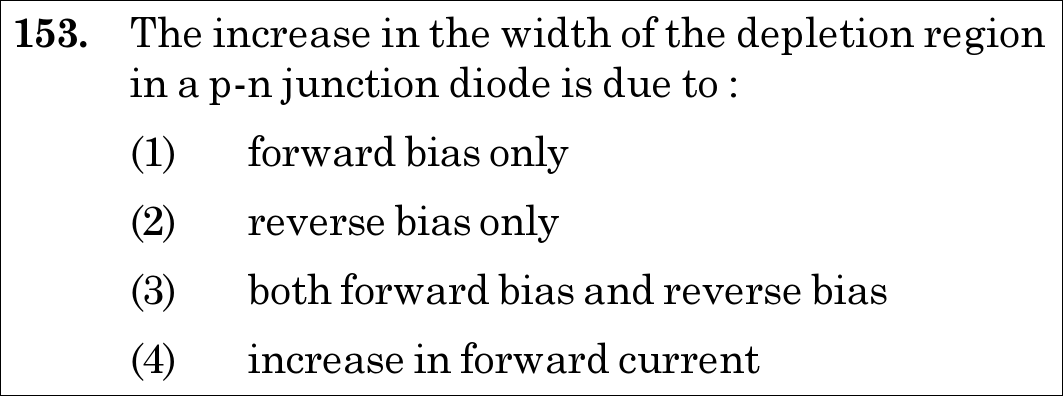
1 forward bias only
2 reverse bias only ✓ Key
3 both forward bias and reverse bias
4 increase in forward current
💡 Verified Solution & 30-Second Hack
✓
Verified Against NTA Final Answer Key
Option (2) : reverse bias only
📚 Semiconductor Electronics: Materials, Devices and Simple Circuits Easy
📋 Given Parameters & Problem Setup
Device p-n junction diode
Observed Change Increase in the width of the depletion region
Question Objective Identify which biasing condition causes this widening
⚡

The 30-Second Exam Hall Shortcut: ⚡ "Forward Bias NARROWS Depletion Layer; Reverse Bias WIDENS Depletion Layer!"

⏱️ 15 seconds

In reverse bias, the positive terminal of the battery is connected to the n-side and the negative terminal to the p-side. This pulls majority charge carriers (electrons in n-side, holes in p-side) AWAY from the junction, uncovering more immobile ionized donor and acceptor ions. Hence, the depletion layer width INCREASES under REVERSE BIAS ONLY! Mark Option (2) in 5 seconds.

1 In forward bias: External field opposes barrier field, pushing majority carriers toward junction -> Depletion layer width DECREASES.
2 In reverse bias: External field aids barrier field, pulling majority carriers away from junction -> Depletion layer width INCREASES.
3 Thus, increase in depletion width occurs under reverse bias only.
4 Select Option (2) reverse bias only.
🛡️
Why You Can 100% Trust This Shortcut: NCERT Physics · Semiconductor Electronics (Semiconductor Diode: p-n Junction under Reverse Bias)
📐

Step-by-Step Rigorous Workflow & Mathematical Proof

Step 1

Structure of the Depletion Region

During the formation of a p-n junction, holes diffuse from the p-side to the n-side and electrons from the n-side to the p-side. This uncovers immobile positively charged donor ions on the n-side and immobile negatively charged acceptor ions on the p-side, establishing a space-charge depletion layer devoid of free charge carriers and setting up an internal barrier electric field directed from n to p.

Step 2

Effect of Reverse Bias

In reverse bias, the p-type region is connected to the negative terminal of the external battery and the n-type region to the positive terminal. The applied reverse voltage produces an external electric field in the SAME direction as the internal barrier field. Consequently, holes in the p-side are pulled away toward the negative terminal, and electrons in the n-side are attracted toward the positive terminal.

Step 3

Consequence on Depletion Width and Barrier Height

Because majority carriers are pulled away from the junction interface, an additional layer of ionized dopant impurity atoms is exposed on both sides of the junction. Therefore, the width of the depletion region increases, and the effective barrier height increases from V0V_0 to (V0+V)(V_0 + V).

Step 4

Contrast with Forward Bias

Under forward bias, the external field opposes the barrier field, pushing majority carriers into the depletion region and dramatically reducing its width.

⭐

360° Option Elimination Engine Key Feature

Diagnose every choice: Know exactly why the right option works and why distractors fail.

4-Option Deep Scan
1 A
✗ Incorrect
Verdict & Scientific Reason:

Incorrect; forward bias DECREASES the width of the depletion layer.

⚠️
Student Fallacy (Why candidates pick this trap): Confusing forward bias with reverse bias effects.
2 B
✓ 100% Correct
Verdict & Scientific Reason:

Factually exact; majority carriers are swept away from the junction, widening the depletion region.

💡
Why this is airtight: None; fundamental semiconductor physics.
3 C
✗ Incorrect
Verdict & Scientific Reason:

Incorrect; forward bias and reverse bias produce opposite effects on depletion width.

⚠️
Student Fallacy (Why candidates pick this trap): Thinking any applied voltage widens the depletion layer.
4 D
✗ Incorrect
Verdict & Scientific Reason:

Incorrect; increase in forward current occurs when the depletion layer is narrowed and overcome, not widened.

⚠️
Student Fallacy (Why candidates pick this trap): Confusing current conduction with barrier widening.
⚠️

NTA Trap Alert: Forward vs Reverse Bias Summary

- Forward Bias: Depletion layer THINS (narrows), Barrier DECREASES, Current FLOWS. - Reverse Bias: Depletion layer WIDENS (thickens), Barrier INCREASES, Current BLOCKED.

🛡️ How to avoid the -1 mark: Widening of depletion region = REVERSE BIAS ONLY!
📖

Core NEET Syllabus Standard

Physics · Semiconductor Electronics: Materials, Devices and Simple Circuits Standard Benchmark
Core Scientific Principle Tested:

""

Syllabus Focus: p-n Junction Diode: Widening of Depletion Region under Reverse Bias
✓ Core NEET UG Syllabus Anchor Syllabus & Academic Standards ↗
NEET 2020 · Q156 Easy
Official NEET 2020 Question 156 - Semiconductor Electronics: Materials, Devices and Simple Circuits
1 Base, emitter and collector regions should have same doping concentrations.
2 Base, emitter and collector regions should have same size.
3 Both emitter junction as well as the collector junction are forward biased.
4 The base region must be very thin and lightly doped. ✓ Key
💡 Verified Solution & 30-Second Hack
✓
Verified Against NTA Final Answer Key
Option (4) : The base region must be very thin and lightly doped.
📚 Semiconductor Electronics: Materials, Devices and Simple Circuits Easy
📋 Given Parameters & Problem Setup
Device Bipolar Junction Transistor (BJT: n-p-n or p-n-p)
Functional Regimes Transistor action in active mode (amplification)
Question Objective Identify the CORRECT statement regarding transistor structural requirements
⚡

The 30-Second Exam Hall Shortcut: ⚡ "Transistor Action: Base Must Be Extremely THIN and LIGHTLY DOPED!"

⏱️ 20 seconds

For proper transistor action, majority carriers emitted by the emitter must pass through the base into the collector without recombining. To minimize base recombination loss (< 5%), the base region MUST BE EXTREMELY THIN (~few micrometers) AND VERY LIGHTLY DOPED! Emitter is heavily doped, collector is moderately doped. Statement (4) is 100% correct! Mark Option (4) in 5 seconds.

1 Doping profile: Emitter (heavily doped) > Collector (moderately doped) > Base (very lightly doped).
2 Physical size: Collector (largest) > Emitter (moderate) > Base (extremely thin).
3 Active bias: Emitter-base is forward biased; Collector-base is reverse biased.
4 Thus, options (1), (2), and (3) are all false.
5 Statement (4) is correct: "The base region must be very thin and lightly doped."
6 Select Option (4).
🛡️
Why You Can 100% Trust This Shortcut: NCERT Physics · Semiconductor Electronics (Bipolar Junction Transistor: Structure and Action)
📐

Step-by-Step Rigorous Workflow & Mathematical Proof

Step 1

Structural Architecture of a Transistor

A junction transistor has three distinct doped regions: 1. Emitter: Supplies majority charge carriers; it is moderately sized and HEAVILY DOPED. 2. Base: The central connecting region; it is EXTREMELY THIN (~few micrometers) and VERY LIGHTLY DOPED. 3. Collector: Collects carriers passing through base; it is physically the LARGEST in size (to dissipate heat) and MODERATELY DOPED.

Step 2

Evaluate Statement (1) and (2)

- Statement (1) claims all regions have same doping: False, doping order is Emitter > Collector > Base. - Statement (2) claims all regions have same size: False, size order is Collector > Emitter > Base.

Step 3

Evaluate Statement (3): Biasing in Active Mode

For normal transistor action (active amplification mode): - The emitter-base junction must be FORWARD BIASED. - The collector-base junction must be REVERSE BIASED. Statement (3) falsely claims both junctions are forward biased (which is the saturation regime, not normal active transistor action).

Step 4

Evaluate Statement (4): Role of Thin, Lightly Doped Base

If the base were thick or heavily doped, most majority carriers injected from the emitter would recombine in the base and never reach the collector. The thin and lightly doped base ensures that only ~2-5% of carriers recombine (IBI_B is very small), allowing >95% to cross into the collector (IC≈IEI_C \approx I_E). Hence, Statement (4) is the defining, correct statement.

⭐

360° Option Elimination Engine Key Feature

Diagnose every choice: Know exactly why the right option works and why distractors fail.

4-Option Deep Scan
1 A
✗ Incorrect
Verdict & Scientific Reason:

Incorrect; doping concentrations are distinctly different (Emitter > Collector > Base).

⚠️
Student Fallacy (Why candidates pick this trap): Assuming symmetric doping across regions.
2 B
✗ Incorrect
Verdict & Scientific Reason:

Incorrect; collector is the largest region to dissipate heat, while base is extremely thin.

⚠️
Student Fallacy (Why candidates pick this trap): Assuming geometric symmetry.
3 C
✗ Incorrect
Verdict & Scientific Reason:

Incorrect; for normal transistor action, the collector junction must be REVERSE BIASED, not forward biased.

⚠️
Student Fallacy (Why candidates pick this trap): Confusing saturation mode with active amplification mode.
4 D
✓ 100% Correct
Verdict & Scientific Reason:

Factually exact; verbatim requirement in NCERT for proper transistor action to allow carrier transit to collector.

💡
Why this is airtight: None; core transistor construction rule.
⚠️

NTA Trap Alert: Transistor Three Regions Cheat Sheet

- Emitter: Moderately sized, Heavily doped. - Base: Very thin, Lightly doped. - Collector: Largest size, Moderately doped. - Biasing in Active Mode: E-B forward biased, C-B reverse biased.

🛡️ How to avoid the -1 mark: Base = THIN + LIGHTLY DOPED (always!).
📖

Core NEET Syllabus Standard

Physics · Semiconductor Electronics: Materials, Devices and Simple Circuits Standard Benchmark
Core Scientific Principle Tested:

""

Syllabus Focus: Transistor Structure Requirements: Base Region Must be Very Thin and Lightly Doped
✓ Core NEET UG Syllabus Anchor Syllabus & Academic Standards ↗
NEET 2020 · Q180 Easy
Official NEET 2020 Question 180 - Semiconductor Electronics: Materials, Devices and Simple Circuits
1 ✓ Key
2
3
4
💡 Verified Solution & 30-Second Hack
✓
Verified Against NTA Final Answer Key
Option (1) : Truth table for AND gate: Output Y is 1 only when A=1 and B=1
📚 Semiconductor Electronics: Materials, Devices and Simple Circuits Easy
📋 Given Parameters & Problem Setup
Input Inverters NOT gates giving A-bar and B-bar
Output Gate NOR gate receiving A-bar and B-bar
⚡

The 30-Second Exam Hall Shortcut: ⚡ "De Morgan Theorem: Y = (A-bar + B-bar)-bar = A · B. The circuit is an AND gate! The truth table outputs 1 only when both inputs are 1. Option (1) / A is the unique match!"

⏱️ 20 seconds

Inputs A and B pass through inverters to yield NOT(A) and NOT(B). These enter a NOR gate, yielding Y = NOT[NOT(A) OR NOT(B)]. By De Morgan's Theorem, NOT(X OR Y) = NOT(X) AND NOT(Y). Here with double negation, Y = A AND B! The circuit is an AND gate, whose truth table has output 1 exclusively when both inputs are 1 (A=1, B=1). Truth table option (1) (Option A) is the exact match!

1 Inputs to NOR gate: A′=AˉA' = \bar{A} and B′=BˉB' = \bar{B}.
2 Output of NOR gate: Y=A′+B′‾=Aˉ+Bˉ‾Y = \overline{A' + B'} = \overline{\bar{A} + \bar{B}}.
3 Apply De Morgan's Law: Y=(Aˉ)‾⋅(Bˉ)‾=A⋅BY = \overline{(\bar{A})} \cdot \overline{(\bar{B})} = A \cdot B.
4 Circuit is a standard 2-input AND gate.
5 Truth table rows: (0,0)->0; (0,1)->0; (1,0)->0; (1,1)->1.
6 Select Option (1).
🛡️
Why You Can 100% Trust This Shortcut: NCERT Physics · Semiconductor Electronics (Digital Electronics and Logic Gates)
📐

Step-by-Step Rigorous Workflow & Mathematical Proof

Step 1

Trace Logic Signals Through the Circuit

- Input AA passes through a NOT gate, producing Aˉ\bar{A}. - Input BB passes through a NOT gate, producing Bˉ\bar{B}. - Signals Aˉ\bar{A} and Bˉ\bar{B} enter a two-input NOR gate.

Step 2

Formulate Boolean Output Expression

The output of a NOR gate is the inverted sum of its inputs: Y=Aˉ+Bˉ‾Y = \overline{\bar{A} + \bar{B}}.

Step 3

Apply De Morgan’s First Theorem

According to De Morgan's Theorem: X+Y‾=Xˉ⋅Yˉ\overline{X + Y} = \bar{X} \cdot \bar{Y}. Letting X=AˉX = \bar{A} and Y=BˉY = \bar{B}: Y=(Aˉ)‾⋅(Bˉ)‾Y = \overline{(\bar{A})} \cdot \overline{(\bar{B})} Since the double inversion of a Boolean variable returns the variable itself (Aˉ‾=A\overline{\bar{A}} = A): Y=A⋅BY = A \cdot B. The composite circuit functions as an AND gate.

Step 4

Construct and Match Truth Table

- When A=0,B=0  ⟹  Y=0⋅0=0A = 0, B = 0 \implies Y = 0 \cdot 0 = 0 - When A=0,B=1  ⟹  Y=0⋅1=0A = 0, B = 1 \implies Y = 0 \cdot 1 = 0 - When A=1,B=0  ⟹  Y=1⋅0=0A = 1, B = 0 \implies Y = 1 \cdot 0 = 0 - When A=1,B=1  ⟹  Y=1⋅1=1A = 1, B = 1 \implies Y = 1 \cdot 1 = 1 This matches Table (1) (Option A).

⭐

360° Option Elimination Engine Key Feature

Diagnose every choice: Know exactly why the right option works and why distractors fail.

4-Option Deep Scan
1 A
✓ 100% Correct
Verdict & Scientific Reason:

Accurate truth table for an AND gate realized by inverting inputs before a NOR gate.

💡
Why this is airtight: None; exact Boolean reduction.
2 B
✗ Incorrect
Verdict & Scientific Reason:

Incorrect; this is the truth table for an OR gate (Y = A + B).

⚠️
Student Fallacy (Why candidates pick this trap): Confusing AND with OR logic.
3 C
✗ Incorrect
Verdict & Scientific Reason:

Incorrect; this is the truth table for a NAND gate.

⚠️
Student Fallacy (Why candidates pick this trap): Adding an extra unintended inversion.
4 D
✗ Incorrect
Verdict & Scientific Reason:

Incorrect; this is the truth table for a basic NOR gate without input inverters.

⚠️
Student Fallacy (Why candidates pick this trap): Ignoring the two input NOT gates.
⚠️

NTA Trap Alert: De Morgan Double Inversion

NOT(NOT A OR NOT B) = A AND B, NOT A OR B. Double negation restores the un-complemented variables.

🛡️ How to avoid the -1 mark: Substitute a test case: A=1, B=1 => inverters give 0, 0 => NOR(0, 0) = 1. Only Table (1) gives 1 for (1,1)!
📖

Core NEET Syllabus Standard

Physics · Semiconductor Electronics: Materials, Devices and Simple Circuits Standard Benchmark
Core Scientific Principle Tested:

""

Syllabus Focus: De Morgan Realization of AND Gate using Inverters and NOR Gate
✓ Core NEET UG Syllabus Anchor Syllabus & Academic Standards ↗

Solve 4 NEET Questions a Day — One per Subject

Cover all 1,140 official NEET questions in 285 days at your own pace. Progress is saved on your device. No login needed.